If you have a related question, please click the "Ask a related question" button in the top right corner. The newly created question will be automatically linked to this question.
TPS25751: Some questions about implementing switching logic control using the TPS25751D
Because of an operation-related issue, only the schematic was submitted. Now ,let me supplement the requried functionality and the issues.
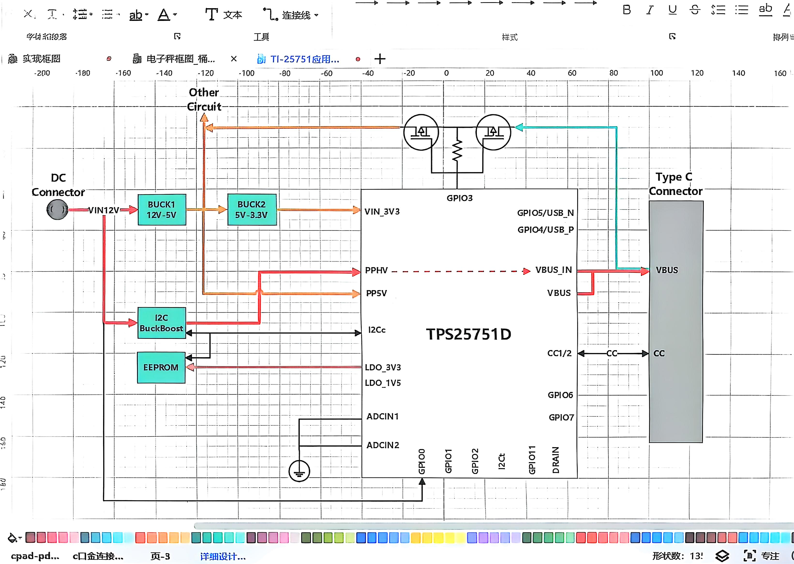
1. After VIN12V is input through the DC connector, VIN12V can be connected to GPIO0 ( or other GPIO) of the TPS25751D through a voltage divider. The TPS25751D uses its ADC function to detect the presence of the 12V input. After that, communication is initiated through the CC pin to negotiate with the Type C connectedf device. The negotiation result should have the TPS25751D acting as the Source, and the Type C connected device acting as the sink.
2. Based on the above, the CC communication also needs to negotiate the power supply voltage and current. The TPS25751D should use the negotiation result to control the I2C-based BUCKBOOST converter to output the corresponding voltage, and enable the internal PPHV path to deliver power to VBUS_IN. [ Qrestion 1: The EVM is currently using a batter charging IC (BQ25798). Is it possible to replace it with a standard one-way output I2C buck-boost converter?]
3. When VIN12V is not inserted into the DC connector,and only a Type-C device is connected, the TPS25751D should support the dead battery mode,where it draws power from the VBUS of the Type-C interface.In this mode, the CC interface must negotiate for the VBUS to supply 5V to the internal system,with a current capability of more than 1.5A.
4. Based on the above "3", the PPHV path switch should be turned off. At the same time, GPIO3 (or another GPIO) should be set to low level to turn on the PFET. (When the PFET is not enabled,the GPIO is in a high-impedance (Hi-Z) state.)
5. Based on points 3 and 4,if VIN12V is inserted into the DC connector at this point, the TPS25751D should quickly detect the 12V input and switch the Type-C device to sink mode, while the TPS25751D becomes the source. After that, the system should operate according to the logic in steps 1 and 2.
Question 2: Please review the above logic point by point to see if it can be implemented as intended. Also, please help to identify whether any of the used pins are inappropriate.
The TPS25751D uses its ADC function to detect the presence of the 12V input. After that, communication is initiated through the CC pin to negotiate with the Type C connectedf device. The negotiation result should have the TPS25751D acting as the Source, and the Type C connected device acting as the sink.
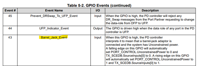
Is there a reason why the customer wants to use the GPIO as an ADC to detect the 12V and not a trigger event? I ask this because there is an GPIO trigger event 'Barrel_Jack_Event' that can be used to monitor the system having unconstrainted power (see picture below).
2.
What are all the necessary voltage/current contracts that the PD controller will source and sink in this design?
Is there a specific I2C buck boost the customer has in mind for this design?
When VIN12V is not inserted into the DC connector,and only a Type-C device is connected, the TPS25751D should support the dead battery mode,where it draws power from the VBUS of the Type-C interface.
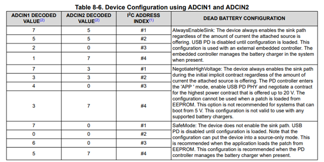
According to the block diagram the dead battery configuration is in Safemode (please see description below). Confirm that this is the correct configuration for their design.
In this mode, the CC interface must negotiate for the VBUS to supply 5V to the internal system,with a current capability of more than 1.5A.
This sink power data object (PDO) of 5V/1.5A can be configured within the GUI under Transmit Sink Capabilities (0x33).
4.
To confirm my understanding, you would like the GPIO to be triggered low when the PD controller is in dead battery mode.
However, please note that the GPIO trigger events are predefined for the TPS25751 and cannot be modified. To determine the specific event that will trigger the GPIO low, I recommend referencingTable 5.2: GPIO Eventsin theTechnical Reference Manual. I suggest considering theAttachedAsSinkevent as a potential trigger. This event may align with the desired behavior of triggering the GPIO low when the device is in dead battery mode.
Could you please confirm with me the GPIO trigger event that will be used in this case.
if VIN12V is inserted into the DC connector at this point, the TPS25751D should quickly detect the 12V input and switch the Type-C device to sink mode, while the TPS25751D becomes the source.
This will go back to my initial comment of whether the 12V input needs to be an ADC detection.
To reiterate, the 'Barrel_Jack_Event' on rising edge will clear the dead battery flag and set the unconstrained power and source inputs fields high or low depending on the rising/falling edge. On rising edge, it also triggers a renegotiation of the connection on the type-c port.