现在是第一次进行OTP,BQ按照你的步骤执行,执行到第11步,等待120ms,读取0x40,返回是0x00,我程序认为是OTP失败退出,然后断电在上电,执行第一步,发现已经写入成功了,请问为什么读取0x40,返回是0x00,我给芯片供电电压是11.5V。和你所给的链接中说的情况不太一致 (If the OTP_WR_CHECK() is returning 0 that indicates the stack voltage is too high for OTP programming)
If you could share a logic analyzer file, that would be helpful to see what exactly was sent and to check if anything potentially occurred during the transaction that may not be obvious.
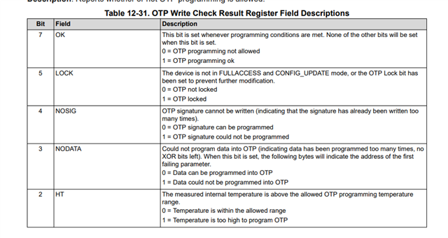
If the OTP_WR_CHECK is reading back 0x00, this would mean that OTP programming is not allowed. What is the stack voltage on the BAT pin when they are trying to program OTP?
When you say the device loses power and reads one of the registers you want to program, did the device truly reset? Is this seen on the REG18 pin where it fully goes to 0V before going back up to ~1.8V?
Also, could you share what registers you wanted to program through a .gg file potentially?