

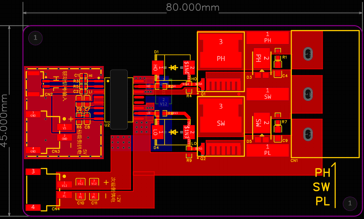
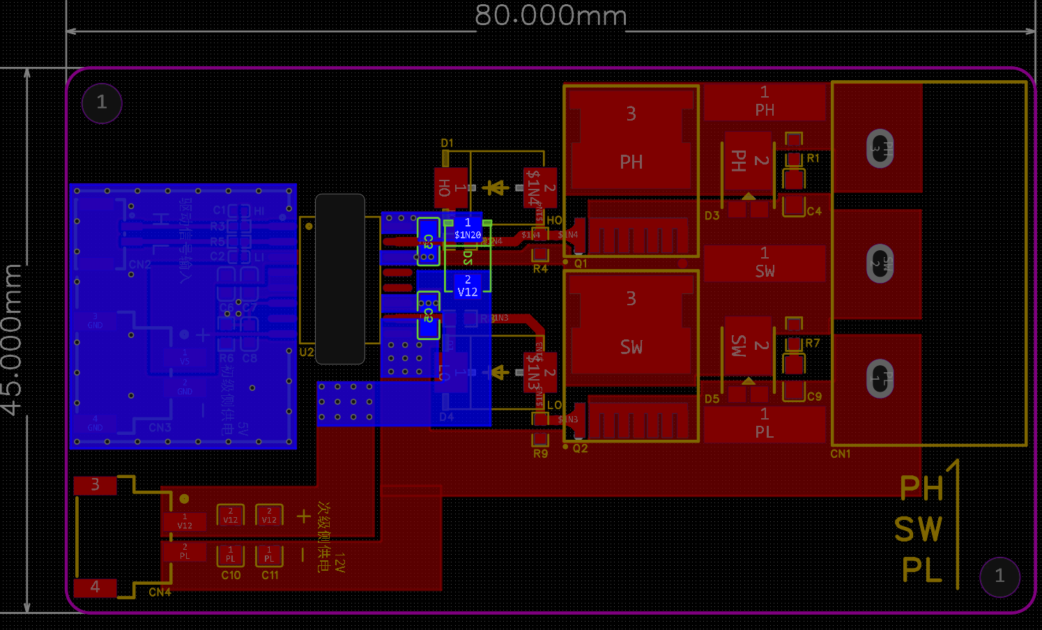
Part Number: UCC21520
参考UCC21520数据手册绘制半桥栅极驱动,但出现较为严重的振铃现象,且二次布局布线后无明显优化效果,请求帮助
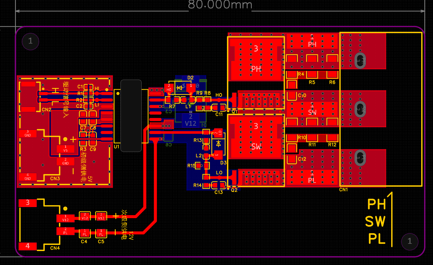
1.第一版Layout与测试波形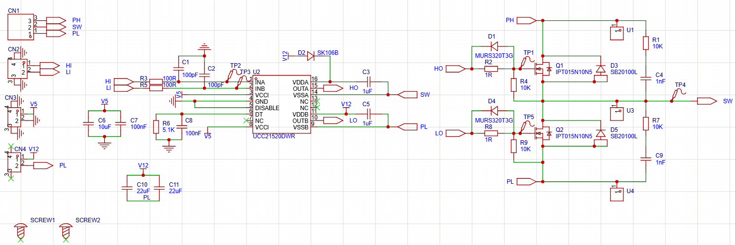

2.第二版设计与测试波形
由于考虑到磁珠在低频下体现电感性,在实际焊接时采用3.3R电阻替代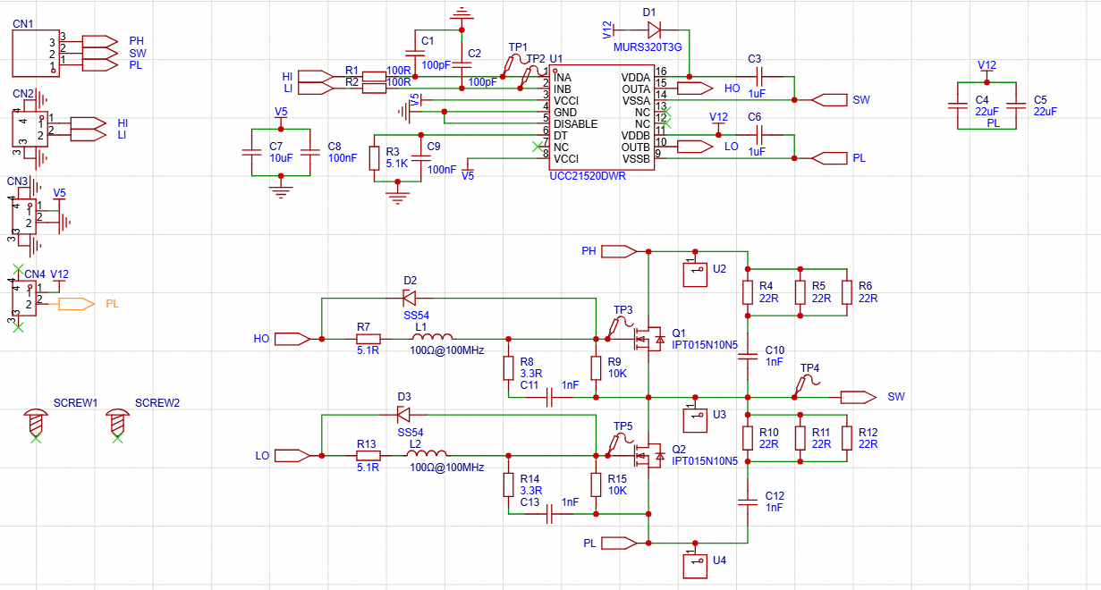

Part Number: UCC21520
参考UCC21520数据手册绘制半桥栅极驱动,但出现较为严重的振铃现象,且二次布局布线后无明显优化效果,请求帮助
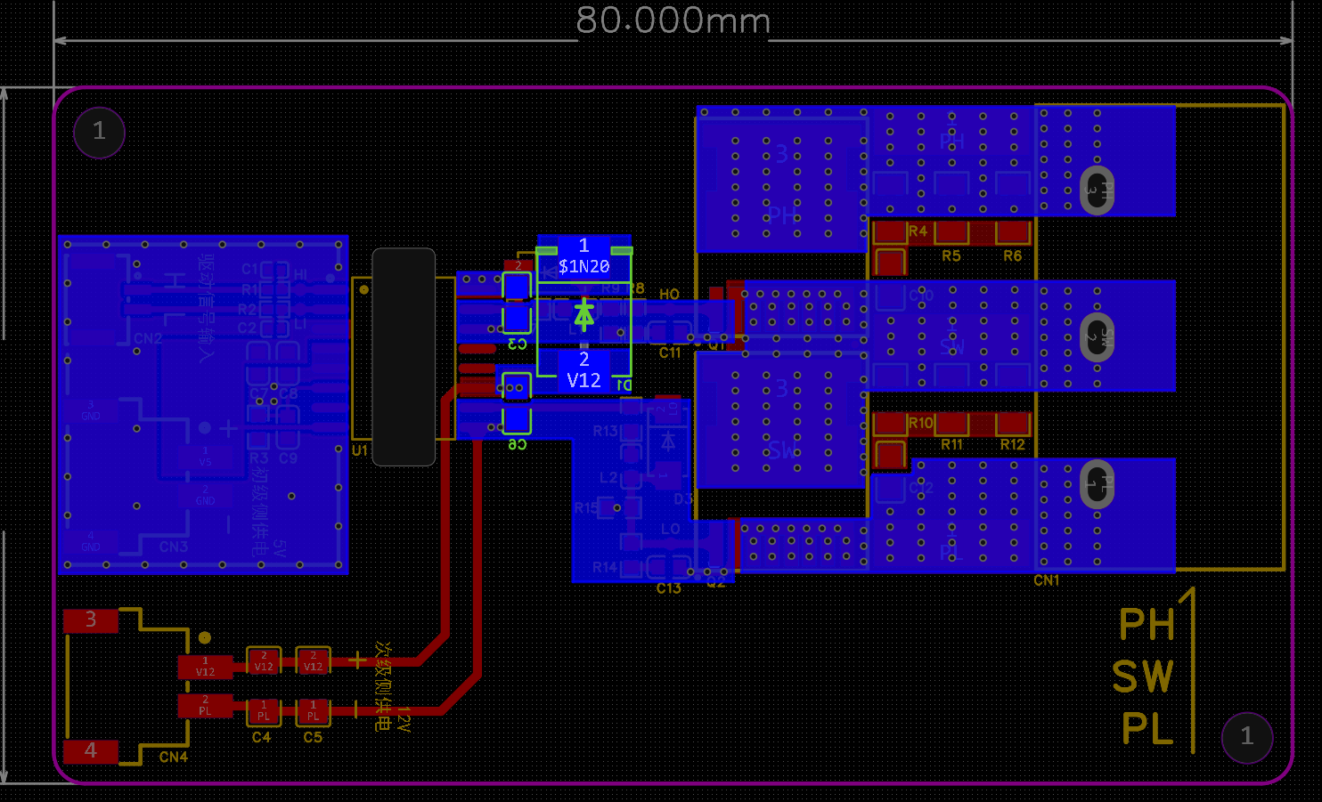
1.第一版Layout与测试波形
2.第二版设计与测试波形
由于考虑到磁珠在低频下体现电感性,在实际焊接时采用3.3R电阻替代
