Part Number: TPS55289
Hi guys,
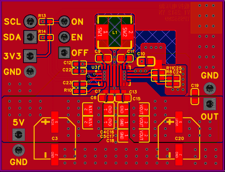
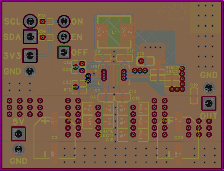
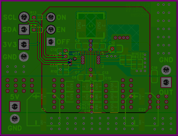
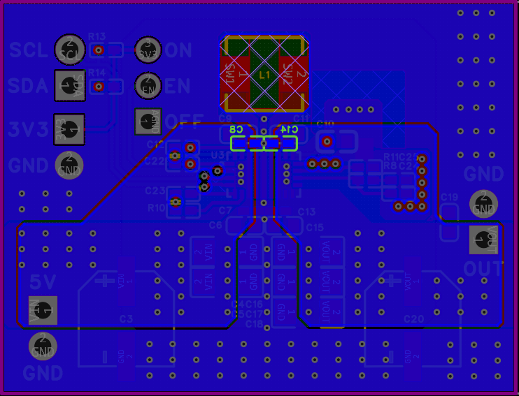
I’m working with the TPS55289 and I’ve run into something a bit odd. I built a small board by basically copying the EVM schematic and layout, and that board works fine. I’ve uploaded both the schematic and PCB here and was hoping someone from TI could take a quick look and see if anything jumps out or looks risky.
The issue shows up on a larger system board, about 20 × 30 cm. On that board, I copied the TPS55289 section exactly from the small board, same layout and routing, no changes. Right now the big board only has the 55289 and its related components populated, nothing else. VIN is coming from a bench supply.
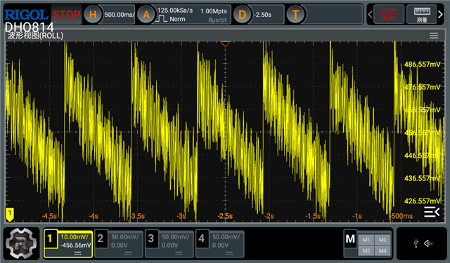
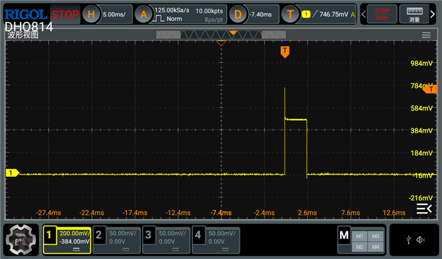
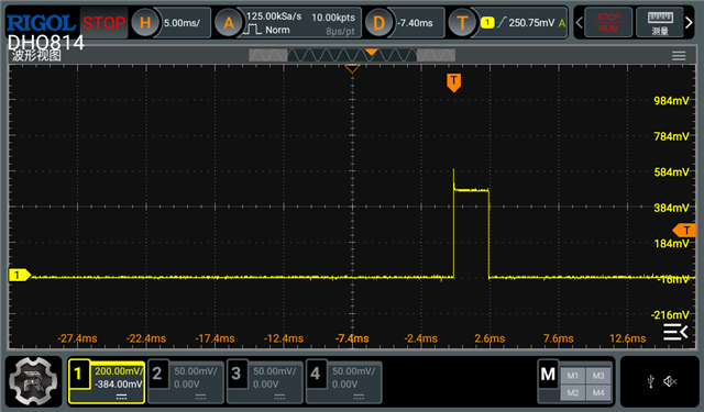
What I’m seeing is that BOOST to SW is about 4.5 V, so the gate drive seems to be there. After I program VOUT over I²C, the output ramps up very quickly, then immediately collapses, and this repeats over and over. At the same time I can clearly hear the inductor “hiccuping.” VIN stays solid the whole time, no droop.
What makes this more confusing is that if I connect the known-good small board to this big board using flying wires, under the same supply and control conditions, the small board works normally. That makes me think it’s not a device or configuration issue, but something related to the big board environment, grounding, or power path.
I wanted to ask if this is a behavior you’ve seen before, or if there are common system-level things to check in this kind of case. For example, could board size, ground impedance, input/output return paths, or something similar cause the 55289 to hit a protection or hiccup mode like this?
I actually have a couple of related questions as well. First is about the FB pin connection when using internal feedback, on the forum that some engineers recommend adding a 100k pull-up from FB to VCC. Is that something that’s needed or recommended in this case?. Second, for the inductor and SW copper, should the GND on inner layers (for example, layer 3) and the bottom layer be cleared out underneath the SW and inductor area? And third, on the input side, would it be reasonable to replace the current input capacitors with three 22uF ceramic capacitors placed close to VIN and PGND?
Thanks in advance for any feedback or suggestions.