Part Number: LM5143
Other Parts Discussed in Thread: CSD18540Q5B, LM5137
Hi,
I am using the LM5143 in a DC/DC converter with an input voltage range 0-60V and an output of 24V. I have conducted a load test under the condition of 36V input and 24V/45A output, and the converter performed well and met all design goals during normal operation.
However, not for long, as the operating temperature increases, the output voltage starts to drift. Eventually, the high-side MOSFET of Channel 2 failed. After removing the failed high-side MOSFET of Channel 2, the remaining Channel 1 works perfectly and can stably output half of the full power of the dual-channel configuration.Is this faliure occur because of high temp?
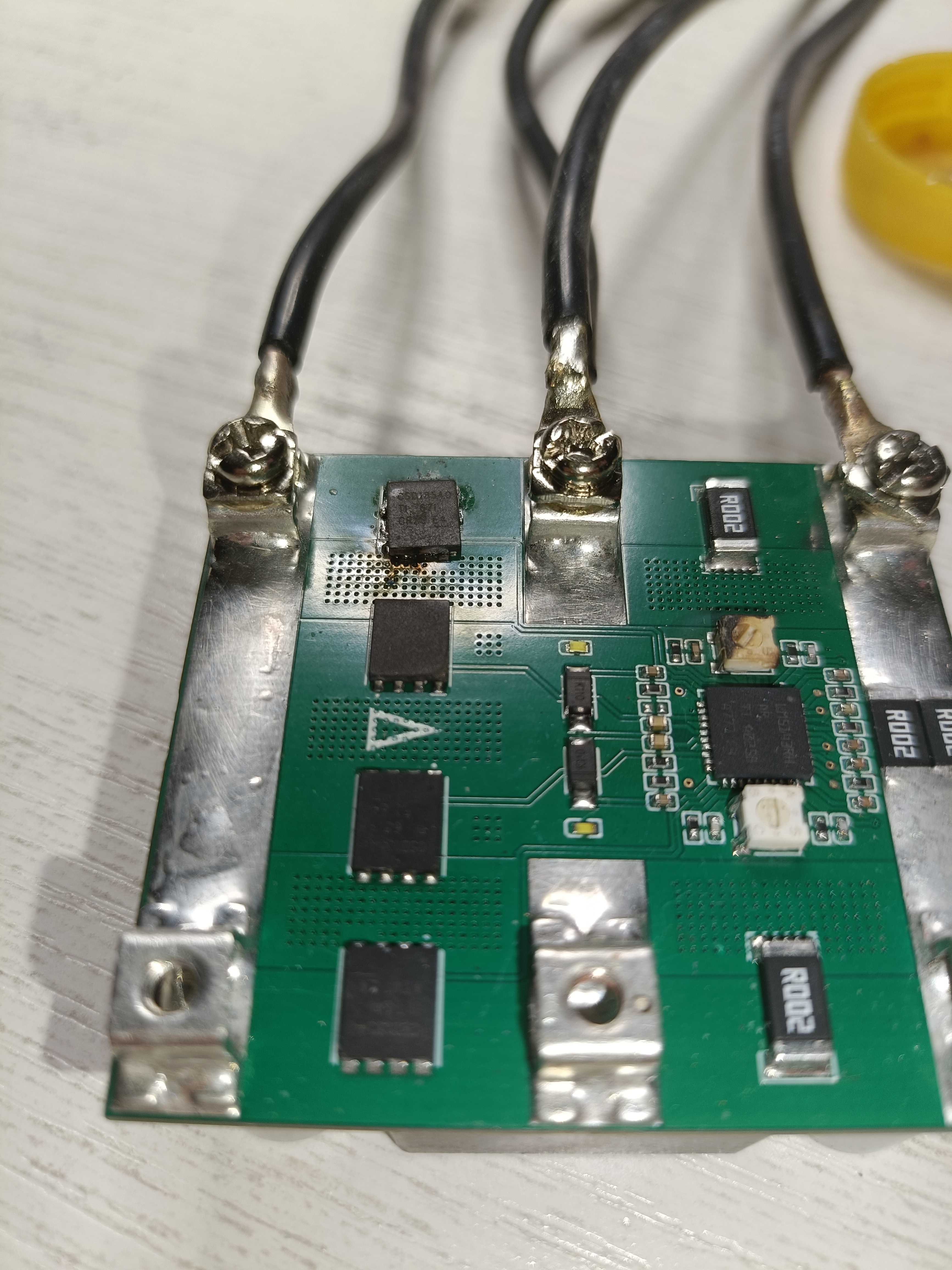
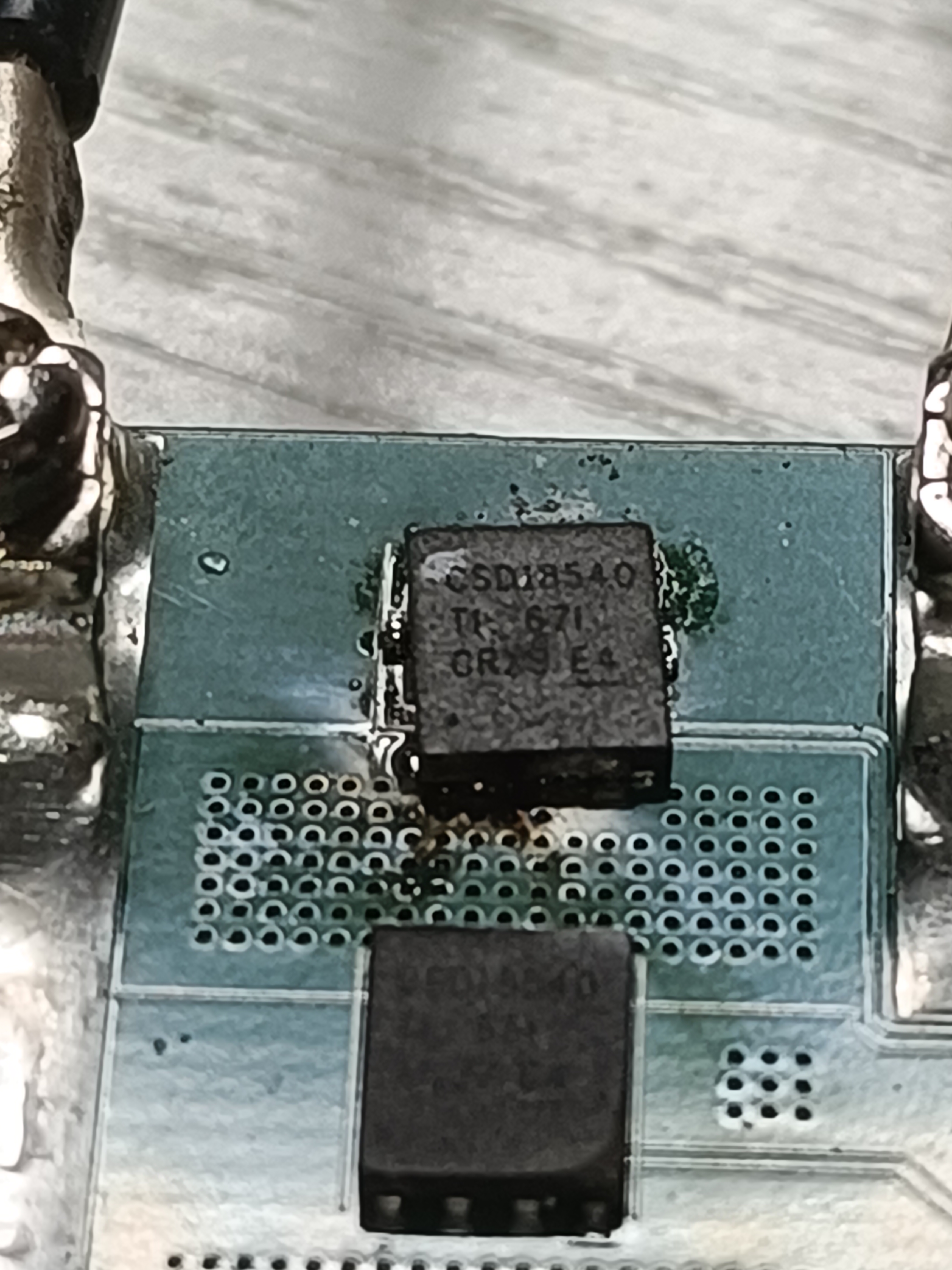
The switch component is CSD18540Q5B. I checked the failed MOSFET with an scope after removal, and the test result showed a short circuit between the G,D,S pins, but I cannot determine the root cause of this failure.Also,when I adjust the feedback potentiometer,sometimes this failure also occurs.
After this, I replaced the failed MOSFET with a new one. When there is no load, the output voltage jumps abnormally (I have verified that the feedback circuit is functioning properly as a votage divider).
Once a load is connected, the new replaced MOSFET immediately becomes extremely hot and shoot-through occurs. I replaced it with another new one again, but the same issue persists: when a 100W light load is connected, the MOSFET gets extremely hot quickly and fails, accompanied by a loud noise. Up to now, this problem has caused the failure of a dozen CSD18540Q5B MOSFETs.
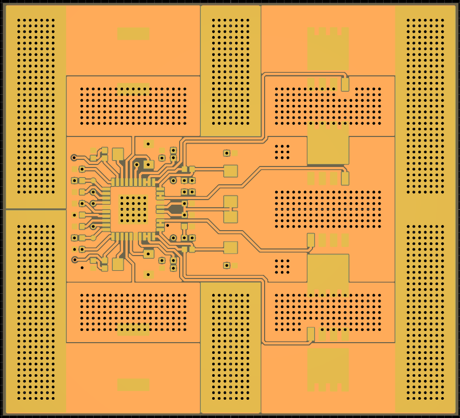
I have attached the schematic and PCB layout of my design for your reference.
Please help me analyze the root cause of this MOSFET failure and the abnormal output voltage issue? Thanks!
Best regards,