UCC25661: The coexistence issue between Normal mode and HF burst mode

Part Number: UCC25661

Hello, engineers from Texas Instruments.
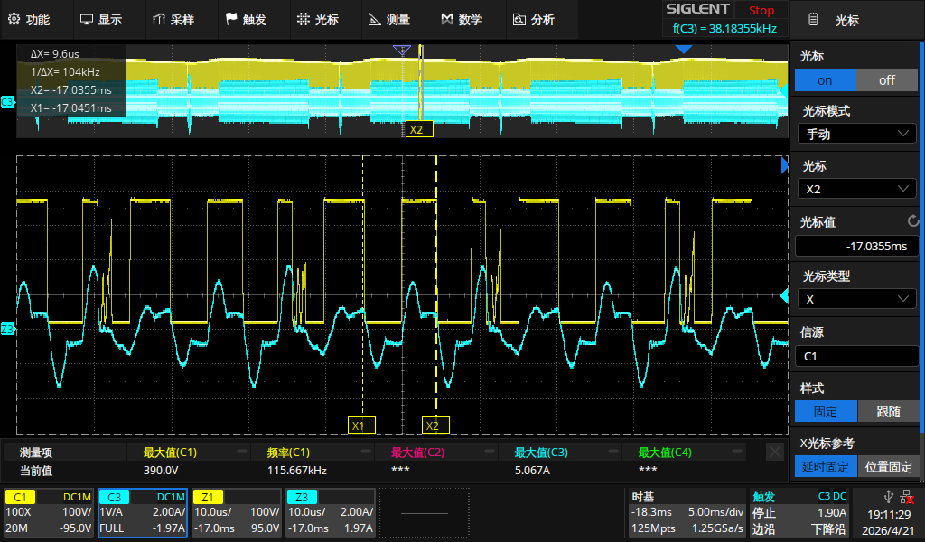
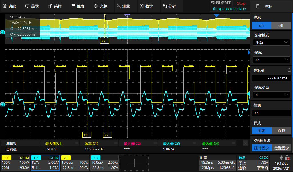
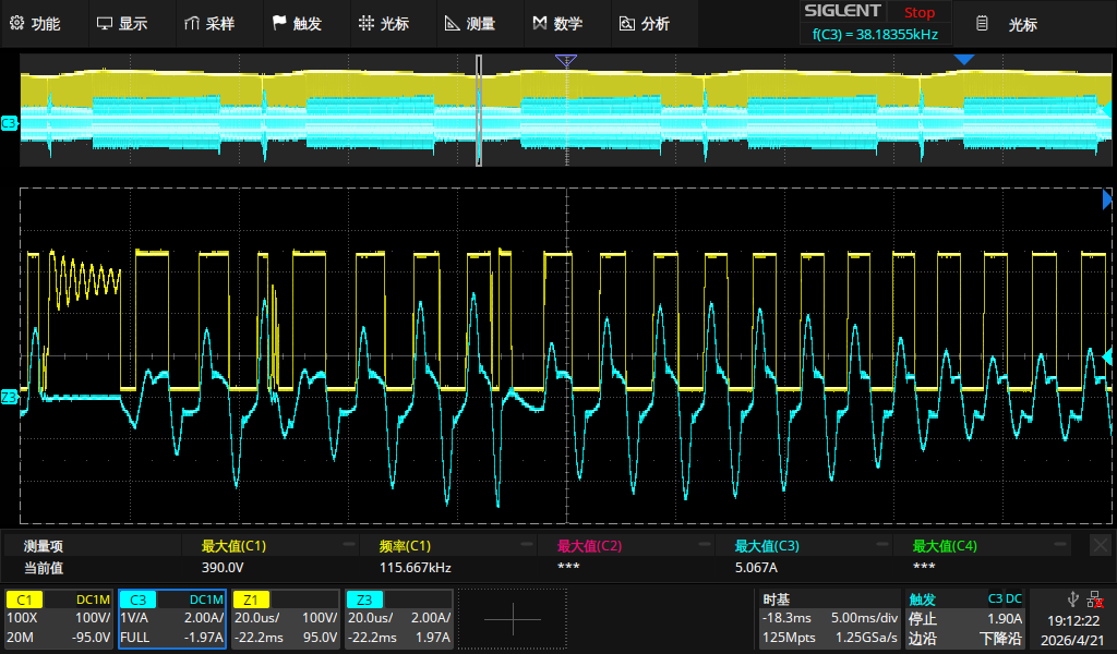
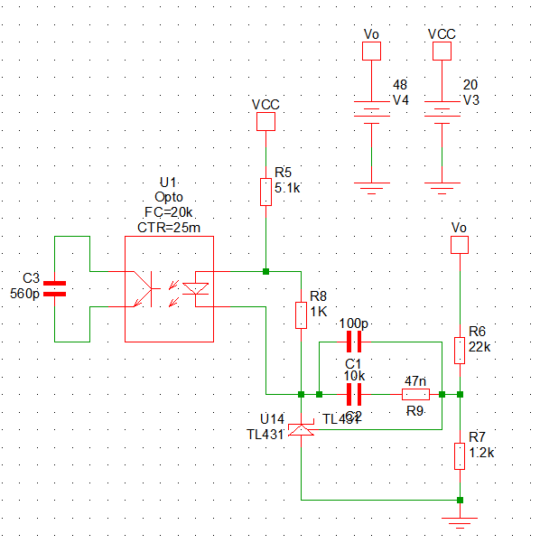
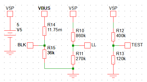
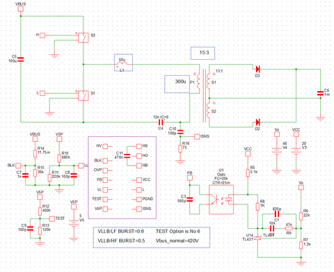
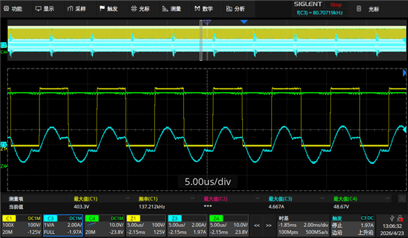
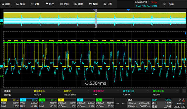
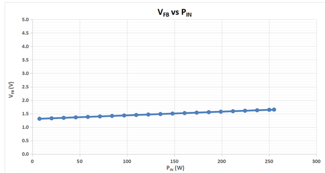
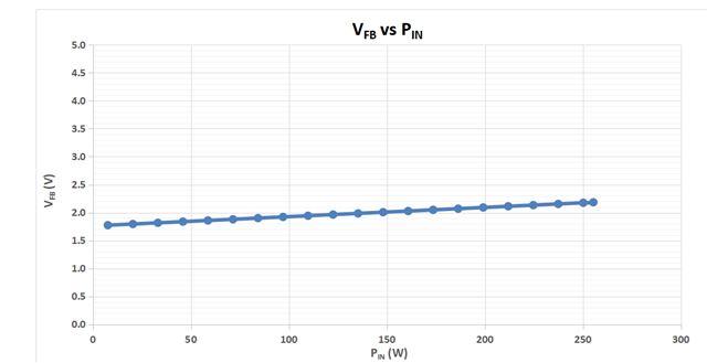
Recently, while working with the UCC25661, I encountered an issue. As the load gradually increases, the power supply exits HF burst mode and is about to enter normal switching mode, during which both modes coexist. Since the hysteresis between HF burst exit and normal switching cannot be manually configured, I would like to ask if you have any good solutions or suggestions.By the way,I also suspected that the issue is caused by the slow loop response, because, as shown in the figure, the current spike occurs at a low frequency. I have also provided the loop parameter diagram I used. Unfortunately, I cannot give the exact value of CTR under this condition, since the current flowing through IF is extremely small. The 0.025 I provided is only an estimated value. 
SDS5104X_PNG_1441.png
SDS5104X_PNG_1442.png
SDS5104X_PNG_1443.png
  • Hello, we have received your case and the investigation will take some time. Thank you for your patience.

  • Thanks for your reply.I would like to add some additional information.I am not using PFC; the circuit is directly powered by an AC supply.The primary turns of the LLC transformer are 15, while both the auxiliary winding and secondary winding have 3 turns each.The chip I am using is the UCC256610.The parameters for the BLK pin, LL pin, and TEST pin are shown in the figure.I would like to clarify that the brown‑in voltage of the LLC is different from the value in the Excel sheet. According to my resistor values, the actual brown‑in voltage of the LLC is 355 V.Moreover, I am unable to plot the curve between Pin and VFB on my own.What I want to express is that the Pin‑versus‑VFB curve in the Excel file is for reference only.The resistor settings for both the LL pin and TEST pin are identical to those in the Excel spreadsheet.

  • In addition, the RISNS resistor I used is not 150Ω but 75Ω. Since the soft start of the UCC256612 cannot be configured, OCP is easily triggered during soft start when a 150Ω resistor is employed.

  • 你好 ,

    能否请您分享一下 UCC25661x 的设计计算器结果(包含您的设计参数)以及原理图?

    看起来你的VFB芯片的Vs引脚曲线没有正确调整。请告诉我你使用的是哪个版本的UCC25661x芯片。

    问候,

    亚米尼。

  • Thank you for your reply. The screenshot below shows the key parameters in the schematic I am using, along with the corresponding design calculation results.

    Item A32 in the calculation table should be 420 V, but I am unable to edit this value in the table. The primary turns of the transformer are 15 and the secondary turns are 3, resulting in a turns ratio of 5, which also cannot be modified in the calculation sheet.Additionally, please disregard cells A254 and A279 in the calculation table. I have not altered these two parameters, as they are irrelevant to the issue I am encountering.

    After further consideration, I suspect the problem may be related to the following factor:Since the unit is directly powered by an AC mains supply, the ripple on the DC bus voltage is relatively large, which leads to the coexistence of HF switching and normal switching.This is because the circuit board is not equipped with a PFC stage.

    Yesterday, I used a 420 V DC power supply to directly feed the DC bus. The captured waveform at full load is attached below, though I am unsure if there is any correlation between the two test conditions; the above is only my preliminary speculation.I currently lean toward loop response issues as the root cause. Unfortunately, I have iteratively adjusted the loop parameters multiple times, yet the problem cannot be effectively resolved.

    The controller I am currently using is UCC256610.

    Thank you for your careful review and support as a TI application engineer.

  • Sorry, I couldn’t find the option to upload the revised form. Actually, I uploaded the spreadsheet at the very beginning of this post, though a few parameters in it hadn’t been updated at that time. Would it be okay if I take a screenshot of the FB curve instead?
  • 你好,

    正如我在之前的回复中提到的,上面的图表是平坦的,据我理解,这就是高频脉冲和正常切换之间波动的原因。

    请将 RBLK 的下限值改为 90kohm,然后检查是否还会出现同样的问题?

    问候,

    亚米尼。

  • 如果只将RBLK下限值改为90K,那意味着LLC的brown in电压会很低。即便曲线可以变陡, 但应用不到实际吧。我修改了TEST引脚部分的电阻,将曲线往上移动,不会再出现两种模式共存的问题。但是我在全功率段调整负载时,发现即便是空载,电源也无法进入LF Burst,这是否意味着,对于曲线而言,最低点太高,而LF Burst的LF Burst Entry点还是小于曲线的最低点,因此电源无法进入LF Burst Entry。

  • 你好,

    请在修改 TSET 设置后分享您的 Vfbreplica 与引脚曲线。

    问候,

    亚米尼。

  • 这种设置下,我的电源不会再存在两种工作模式并存的现象。但正如我之前提到的,电源无法进入LFBurst,是否和LF Burst Entry这个电压太高有关?

    另外,我的电源是240W的,我的曲线在满载的时候,FB只有2.3V,其实这个值是偏小的对吧,意味着OPP的时候功率会很大。

  • 你好,

    您的系统是否仅在轻负载下以高频脉冲串模式运行?

    请分享设计计算器中的LL引脚设置部分。

    此外,我的电源是 240W 的,我的曲线显示满载时 FB 电压只有 2.3V。这个值实际上偏低,这意味着启用 OPP 模式后功耗会非常高。

    你的OPP极限值与你的功率水平相差甚远。

    你需要选择合适的BLK引脚电阻,使得在标称输入电压下,BLK引脚上的等效电压约为4V。(因为UCC256610和UCC256614的扩展增益范围功能已启用)。否则,你的Vfbreplica与引脚关系图将呈直线,并且你会看到控制器在正常模式和突发模式之间来回摆动。

    正如我之前提到的,由于所选部件具有 EGR 功能,因此您还需要更换 BLK 电阻器。

    请发送更新后的设计计算器。

    问候,

    亚米尼。

  • "你的系统是否仅在轻负载下以HF Burst模式运行":是的。如果负载更轻,我希望系统会从HF Burst切换到LF Burst。但目前即便是空载,系统也不会进入LF Burst。

    你好,这是我的LL设置部分。我很想知道为什么要把VLLB/LF Burst设置成固定的0.6?这意味着VLLB/HF Burst的值必须要小于0.6,表格里仅有0.55 0.5 0.45这三种选项。

    对于BLK电阻的选择,我目前使用的upper电阻是11.75M,lower电阻是36K。实在抱歉,我想了很久,也没有明白你说的“使得在标称输入电压下,BLK引脚上的等效电压约为4V。(因为EGR功能)”确定4V没有打错吗?

  • 你好,

    在相同的输入电压下,启用 EGR 的版本比未启用 EGR 的版本增益更高,因为 BLK 会与 TSET 和 ISNS 一起影响增益。

    通常,我们选择 BLK 电阻时,会确保标称输入电压下的 VBLK 约为 1.5V。但对于 UCC256610 和 UCC256614,我们选择 BLK 电阻时,会确保 BVLK 约为 4V。

    你需要提高突发阈值才能进入低频突发模式。

    您分享了LO的波形。

    VLLB/LF 内部已固定,以便于选择 LL 引脚电阻。是的,您需要在 0.5、0.55 和 0.45 之间选择一个电阻值,才能同时获得高频和低频脉冲。

    问候,

    亚米尼。

  • Sorry for the late reply. I just got back from the Labor Day holiday, wish you happiness every day.

    Given the EGR function of the UCC256610, does this mean it can support a lower input voltage?

    Really sorry. I still don’t quite understand why the voltage on the BLK pin you mentioned is around 4V. I’ve taken a screenshot of my calculation process for the BLK resistor. Could you please help check where I made a mistake and where exactly this 4V comes into play?

    For the UCC256610,VBLK_stop=1V ,VBLKstart_hys=0.05V,IBLK_sink=1uA;

    RBLK_upper=11.8M,RBLK_lower=36K 。According to the datasheet, the calculation process is as follows.

    Do you mean the voltage of VBLK_start should be 4V?

    Thank you so much for your help these days. Thanks again!

  • What you mean should be: When the PFC is operating normally, the VBLK voltage should be 4V instead of 1.5V. That’s why you previously suggested changing RBLKupper to 90kΩ. The calculations for RBLKupper at 36kΩ and 90kΩ are as follows. However, there is an issue when RBLK is set to 90kΩ: the Vbrown_in voltage will become very low. Will this cause any problem when applied in the LLC topology? The loop gain will be extremely high under this condition.

  • 您的意思是:当 PFC 正常工作时,VBLK 电压应为 4V 而不是 1.5V。这就是您之前建议将 RBLKupper 改为 90kΩ 的原因。RBLKupper 在 36kΩ 和 90kΩ 时的计算如下。但是,当 RBLK 设置为 90kΩ 时存在一个问题:Vbrown_in 电压会变得非常低。这在 LLC 拓扑中应用时会造成什么问题吗?在这种情况下,环路增益会非常高。