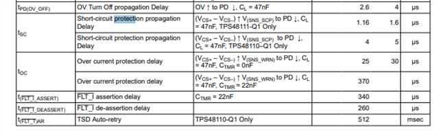
TPS4811-Q1: 关于TPS48111的短路保护

Part Number: TPS4811-Q1

我们用TPS48111实现一个预充及主开关的功能。并联了5个TOLL封装NMOS。电池为15串,54V电池。负载一般在20A一下,但瞬时电流有可能到达200、300A。

图中R250实际贴的是3.6K,C257实际为100K。以实现一个315A、Latch-off的短路保护。
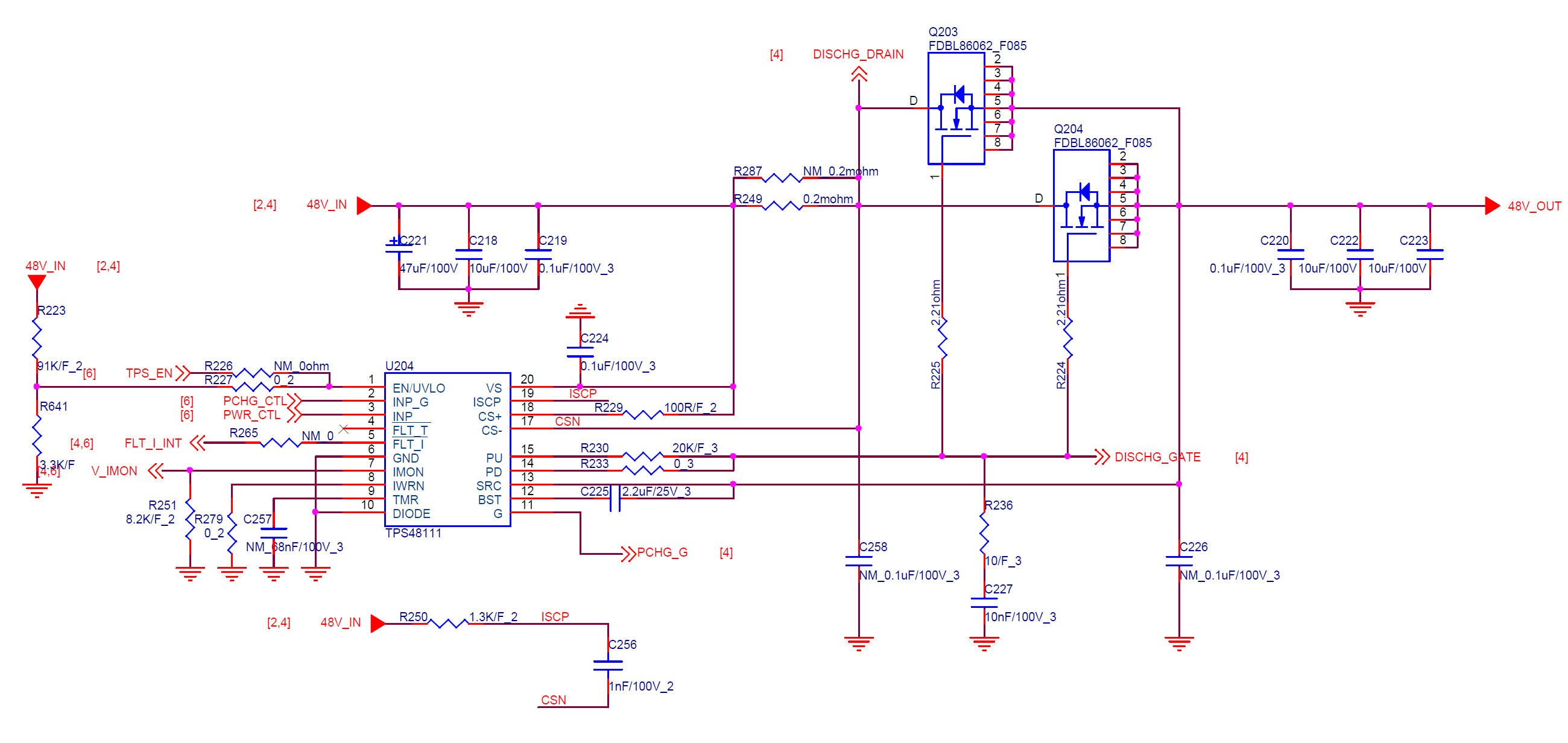
想请问一下,
(1)如果在电流超过315A时,芯片保护瞬间,是否有可能损坏MOS或者TPS芯片?需要对MOS、对TPS48111芯片做哪些保护措施吗?

(2)如果48V_IN处的电压迅速从0升到电池电压(50V、60V),为防止这个大的dv/dt导致Q203等MOS的误导通,需要加电容在G到GND之间,还是G、S之间?
 非常感谢!

  • 您好,收到了您的案例,调查需要些时间,感您的耐心等待。

  • 您好

    如果在电流超过315A时,芯片保护瞬间,是否有可能损坏MOS或者TPS芯片?

    最好是存在保护电路。

    需要对MOS、对TPS48111芯片做哪些保护措施吗?

    缓冲电路——防止瞬间过流,泄流电路——当电流经过缓冲后来保证适当泄放避免大流量持续的影响。过流保护电路——防止突破以上极限对于IC造成损伤。

    如果48V_IN处的电压迅速从0升到电池电压(50V、60V),为防止这个大的dv/dt导致Q203等MOS的误导通,需要加电容在G到GND之间,还是G、S之间?

    两个部分均要做适当保护,但从您这个问题建议加载G-GND 之间做适当缓冲泄放,G-S要存在过流和误导通的保护处理(比如过流或者是错误导通对于后续的影响)

    TPS4811-Q1: Enhanced transient voltage protection - Power management forum - Power management - TI E2E support forums

  • Hi,Daniel

           请问下,

           1)当短路保护值设在300A左右时,设计上有什么要注意的吗?芯片是否会准确的在300A左右动作,进行保护?

           2)当短路保护值设在300A左右时,输出和GND之间如果放一个或几个续流二极管,这个二极管需要什么规格?If(av)或者If(瞬时)大概需要多少合适?

           3)我看规格书上说,输出保护可以放续流二极管,也可以放TVS。单放TVS是否可以?能起到续流二极管的作用吗?

           4)两个部分均要做适当保护,但从您这个问题建议加载G-GND 之间做适当缓冲泄放,G-S要存在过流和误导通的保护处理(比如过流或者是错误导通对于后续的影响)  ------------G-GND之间是只加一个电容,还是加电阻串电容?G、S之间具体如何保护?是加一颗电容吗?

           非常感谢!


  • 您好

       1)当短路保护值设在300A左右时,设计上有什么要注意的吗?芯片是否会准确的在300A左右动作,进行保护?

           2)当短路保护值设在300A左右时,输出和GND之间如果放一个或几个续流二极管,这个二极管需要什么规格?If(av)或者If(瞬时)大概需要多少合适?

    根据datasheet说明会存在延迟,建议参考官方资料和延迟酌情匹配。

     3)我看规格书上说,输出保护可以放续流二极管,也可以放TVS。单放TVS是否可以?能起到续流二极管的作用吗?

    9.5 Power Supply and EMI Recommendations When the external MOSFETs turn OFF during the conditions such as INP control, overvoltage cutoff, overcurrent protection causing an interruption of the current flow, the input parasitic line inductance generates a positive voltage spike on the input and output parasitic inductance generates a negative voltage spike on the output. The peak amplitude of voltage spikes (transients) depends on the value of inductance in series to the input or output of the device. These transients can exceed the Absolute Maximum Ratings of the device if steps are not taken to address the issue. Typical methods for addressing transients include: • Use of a TVS diode and input capacitor filter combination across input to and GND to absorb the energy and dampen the positive transients. • Use of a diode or a TVS diode across the output and GND to absorb negative spikes. The TPS4811Q1 gets powered from the VS pin. Voltage at this pin must be maintained above V(VS_PORR) level to ensure proper operation. If the input power supply source is noisy with transients, then TI recommends to place a RVS - CVS filter between the input supply line and VS pin to filter out the supply noise. TI recommends RVS value around 100Ω. In case where large di/dt is involved, the system and layout parasitic inductances can generate large differential signal voltages between ISCP and CS- pins. This action can trigger false short-circuit protection and nuisance trips in the system. To overcome such scenario, TI recommends to add filter capacitor of 1nF (CSCP) across ISCP and CS- pins close to the device. Because nuisance trips are dependent on the system and layout parasitics, TI recommends to test the design in a real system and tweaked as necessary. The following figure shows the circuit implementation with optional protection components.

    请您参考这部分说明。

     4)两个部分均要做适当保护,但从您这个问题建议加载G-GND 之间做适当缓冲泄放,G-S要存在过流和误导通的保护处理(比如过流或者是错误导通对于后续的影响)  ------------G-GND之间是只加一个电容,还是加电阻串电容?G、S之间具体如何保护?是加一颗电容吗?

    9.6.1 Layout Guidelines

    请您参考这个部分说明进行酌情添加适合您的相关阻容。

  • Hi,Daniel

             还有个问题,如果我既不想有过流保护,也不想有短路保护,TPS48111支持这种模式吗?我该如何配置TPS48111?

             目前, 我将C256改为0欧姆电阻,将ISCP和CS-短接;TMR接0欧姆电阻接GND;将R250移开,将ISCP和VS断开。

             不过这么接,貌似TPS48111不工作,是不是接的不对。

  • 您好

    不建议您如此操作,如果您坚持官方没有相关推荐建议。

  • 好的。就是过流保护或者短路保护两者必需选一种。那如果我把过流保护的时间设置的长一些,例如300ms,甚至4s、5s,这是可以靠增大TMR电容实现的吧?

    另外TMR上的电容耐压需要多少?我看到TMR对GND的最大电压为5.5V,是不是理论上16V耐压的电容就行。不过我看到EVM上选的TMR电容的耐压分别为50V和100V,我确认一下。