This thread has been locked.
If you have a related question, please click the "Ask a related question" button in the top right corner. The newly created question will be automatically linked to this question.
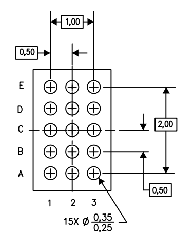
BQ27546芯片是15引脚的BGA封装,该封装引脚与引脚之间的间距小于10mil,无法在Altium Designer进行电气走线,请问中间的引脚如何走线呢?能否引脚的焊盘设置为通孔,在Bottom Layer层引出?
可参考其他CSP封装的EVM走线
两个圆形焊盘圆心之间的距离是0.5mm,但是去掉两圆心之间的直径,边缘相距0.25mm,大概是9.8mil,这种间距是无法走线的,那如何处理中间一排的引脚走线问题?


