This thread has been locked.
If you have a related question, please click the "Ask a related question" button in the top right corner. The newly created question will be automatically linked to this question.
Dear TI:
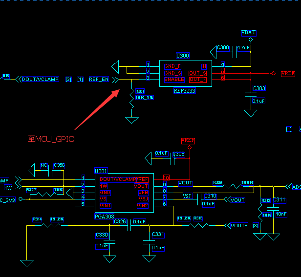
我们在使用REF3233芯片3.3V基准电压给ADC供电时(空载状态)输出电压偏差太大,有时电压为3.294V,有时电压为3.28V,也有出现只有3.26V,,输入电压为3.8V。EN使能脚接的MCU的GPIO口(电平为3.3V),REF3233是否有上电时序要求?这个为什么会影响电压输出偏差大?
之前有看过datasheet Figure 23和 Table 1,但对ENABLE上电时间要求理解不是太清楚,是否ENABLE和Vin的上电时间要在2ms以内?这样是否就不能用MCU的GPIO控制ENABLE(大部分MCU初始化完要10ms以上)?要改用VIN加RC电路上拉ENABLE pin?