

看到我理解的机制是否正确??????????
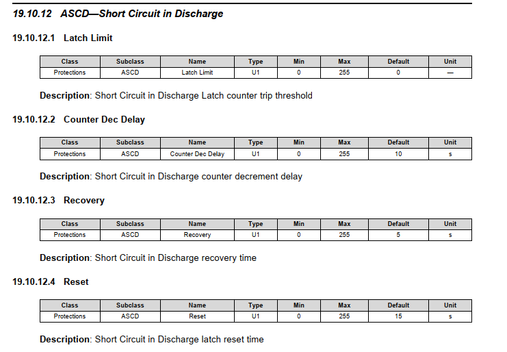
In general, when a fault is detected after the Delay time, the CHG and DSG FETs will be disabled (Trip stage), and an internal fault counter will be incremented (Alert stage). Since both FETs are off, the current will drop to 0 mA. After Recovery time, the CHG and DSG FETs will be turned on again (Recovery stage).
If the alert is caused by a current spike, the fault count will be decremented after Counter Dec Delay time. If this is a persistent faulty condition, the device will enter the Trip stage after Delay time, and repeat the Trip/Latch Alert/Recovery cycle. The internal fault counter is incremented every time the device goes through the Trip/Latch Alert/Recovery cycle. Once the internal fault counter hits the Latch Limit, the protection enters a Latch stage and the fault will only be cleared through the Latch Reset condition.
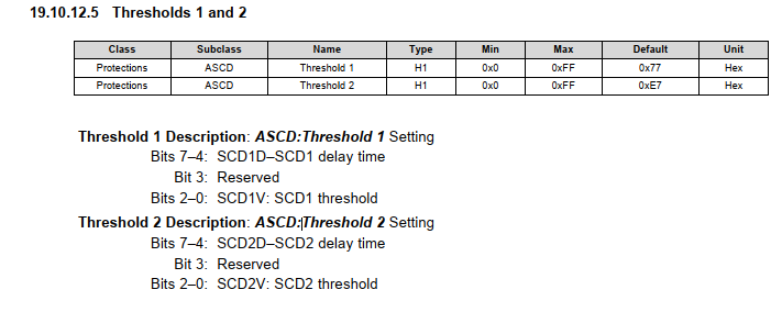
根据上述的资料,当触发短路保护阀值时,在(Bits 7–4: SCD1D–SCD1 delay time)的延迟时间后触发短路保护,关闭FET。在Recovery 延迟时间后,尝试打开FET。如果是电流尖峰引起的,则在Counter Dec Delay延迟时间后,计数器递减。如果是持续的短路状态,将在(Bits 7–4: SCD1D–SCD1 delay time)的延迟时间后继续触发短路保护,内部计数器会递增,,当递增到Latch Limi限制后,彻底锁存。只有达到RESET的复位时间后,才会再次触发短路保护。

