This thread has been locked.
If you have a related question, please click the "Ask a related question" button in the top right corner. The newly created question will be automatically linked to this question.
TI工程师你好!
我目前打算使用LM25118设计线路,关于LAYOUT希望能得到一些建议。
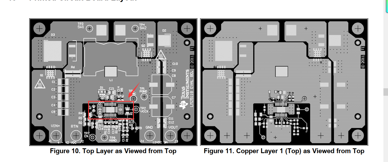
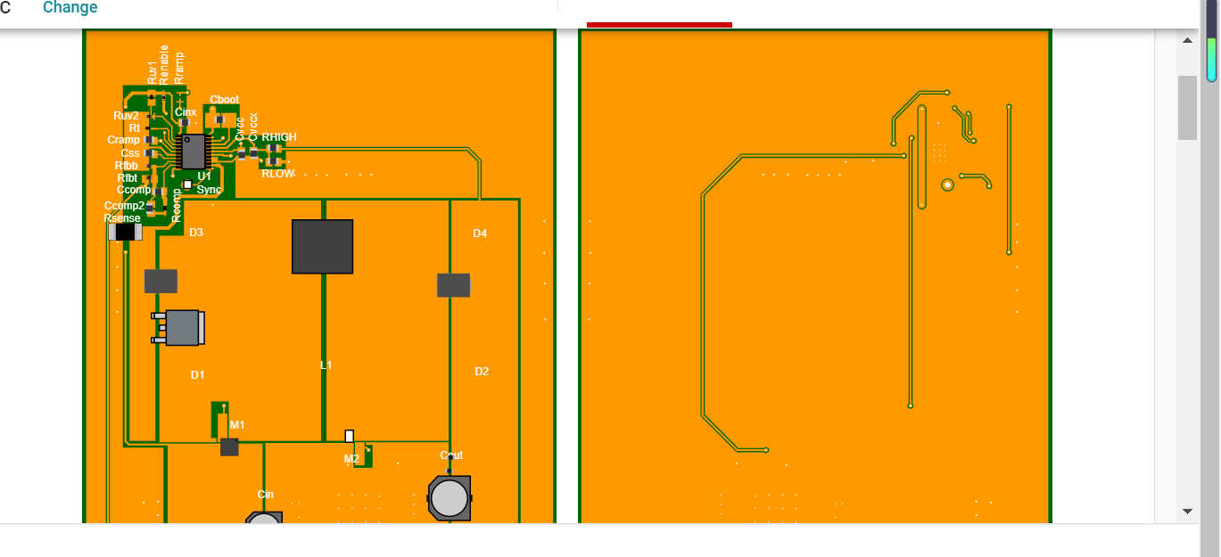
下图是DEMO板的PCB设计 12V/3A 。使用的是四层板 但是芯片的下侧只敷了一小块铜(见图1标记处)。而且只是通过过孔将内层也连接了和表层一样大面积的敷铜。并没有与内层的大块GND连接到一起,这样设计是否会影响芯片的散热效果?是否可以将芯片下侧的敷铜在与内层大面积的地连接到一起。谢谢!
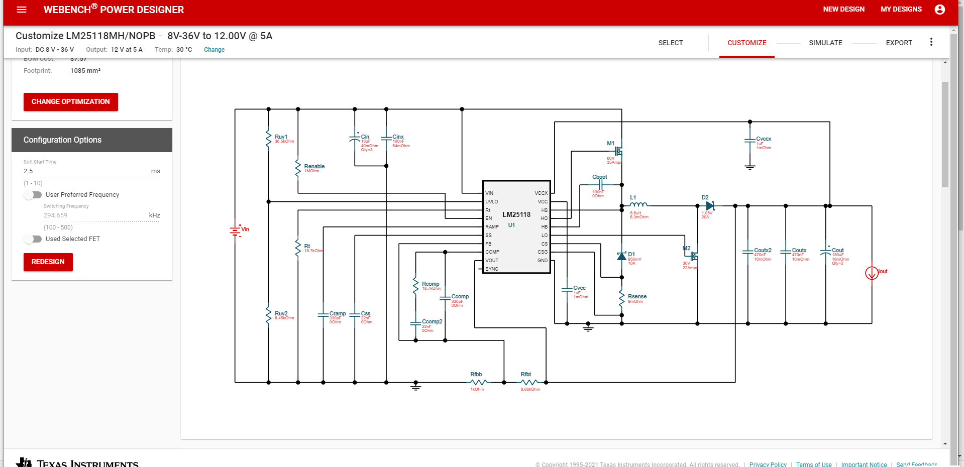
TAO工你好!感谢你的答复。我有几个问题还想咨询一下,就是我使用WEBENCH设计生成的电路是可以直接使用的吧?还有就是参考电路建议使用的元器件也是可以直接用的吧?参考电路生成的PCB用的是两层板 可以用两层是?
就是WEBENCH生成的原理图和PCB根本对不上。PCB上能看到场管M1但是M2压根也没有,PCB上有D3,D4 原理图上压根也没有,原理图上D2是插件的 ,PCB上也看不出来。
Hi
四层板也没有问题的。