Hi all:
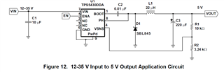
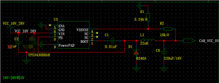
设计原理图 schematic diagram:
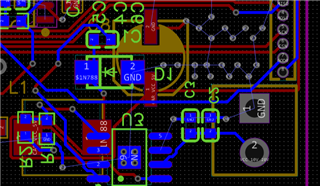
PCB图片:
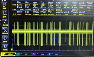
示波器图片 image signal on oscilloscope:
我需要大家的帮助,感谢!
I need your help and advice.
Thank&Regard
Hi all:
设计原理图 schematic diagram:
PCB图片:
示波器图片 image signal on oscilloscope:
我需要大家的帮助,感谢!
I need your help and advice.
Thank&Regard