Other Parts Discussed in Thread: LM25141
Author: fusai.lin@thundersoft.com
Application: ADAS Power module
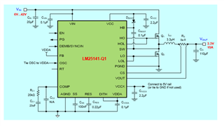
1. The circuit is as below:
UGBATT=12V,
SOM_3V3_Enable=3.3V
2.Abnormal phenomenon des as below:
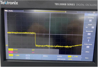
while the load is empty, the bulk output votlage is 3.3V (normal), while the load is above 10mA, the ouptut votlage is shut down , then remove the load , the output votlage is rise up to 3.3V slowly about 10s.
We test the case as below:
1,OSC connect to Ground and connect to 5V
2,Current sense is enable and disable(5mR current sense resistor short ,CS and VOUT unused)
3,VCCX connect to Ground and connect to Vout
the result phenomenon is the same.
Test data as below:
|
LM25141 |
definition |
request |
test (V) |
|
1 |
DEMB |
5 |
|
|
2 |
VDDA |
5 |
|
|
3 |
AGND |
0 |
|
|
4 |
RT |
1.25 |
|
|
5 |
DITH |
5 |
|
|
6 |
OSC |
0 |
|
|
7 |
LOL |
abnormal |
|
|
8 |
LO |
abnormal |
|
|
9 |
PGND |
0 |
|
|
10 |
VCC |
5 |
|
|
11 |
HB |
abnormal |
|
|
12 |
SW |
abnormal |
|
|
13 |
HO |
abnormal |
|
|
14 |
HOL |
abnormal |
|
|
15 |
VIN |
12 |
|
|
16 |
VCCX |
0 |
|
|
17 |
VOUT |
unused |
|
|
18 |
CS |
unused |
|
|
19 |
FB |
5 |
|
|
20 |
COMP |
||
|
21 |
PG |
0 |
|
|
22 |
SS |
0 |
|
|
23 |
EN |
3.3 |
|
|
24 |
RES |
3. The Vout output waveform:
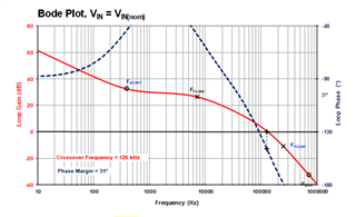
4. The bode plot
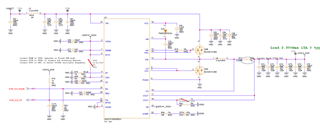
5. The simulation circuit