你好
想請問目前開發階段使用BQ769142,

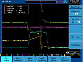
做短路測試時量測波型如下圖:
1.黃色:Q8 DFET VGS電壓
2.藍綠色:負載電流
3.粉紅色: MCU 3.3V電源
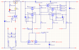
1.綠色:量測電路圖上的CD點位置

測試結果在上述量測地方都會產生很大的振鈴,有辦法解決使振鈴變小嗎?
在幫忙協助回答。
謝謝
This thread has been locked.
If you have a related question, please click the "Ask a related question" button in the top right corner. The newly created question will be automatically linked to this question.
你好
想請問目前開發階段使用BQ769142,

做短路測試時量測波型如下圖:
1.黃色:Q8 DFET VGS電壓
2.藍綠色:負載電流
3.粉紅色: MCU 3.3V電源
1.綠色:量測電路圖上的CD點位置

測試結果在上述量測地方都會產生很大的振鈴,有辦法解決使振鈴變小嗎?
在幫忙協助回答。
謝謝
您好,请参考下面的内容
Parallel FET oscillation. Some FETs will work well when connected directly in parallel, some need some gate isolation to avoid oscillation. As one FET turns off it sheds load to another which then dumps its load back to the others which results in a high frequency oscillation which can result in large voltages and damage. When this is described in industry literature, it is often recommended to use a small individual gate resistance perhaps 10% of the total resistance or a ferrite bead to isolate the gates to suppress the oscillation. This allows the gates to receive about the same drive signal but have enough isolation to prevent oscillation. In several designs where we have used the CSD FETs in parallel we needed to use beads or small resistors to prevent oscillation. Check your design/schematic, inspect the gate signals during switching. Note that a probe on a gate can alter the circuit. When providing isolation it is good to follow the guideline to maintain most of the drive resistance as a common value so the FETs switch at the same time. If completely separate resistances are used from the driver component tolerances could allow the parallel FET to turn off at different times resulting in the last FET to switch off to have the full short circuit load, that FET might be overstressed in that situation and fail.