

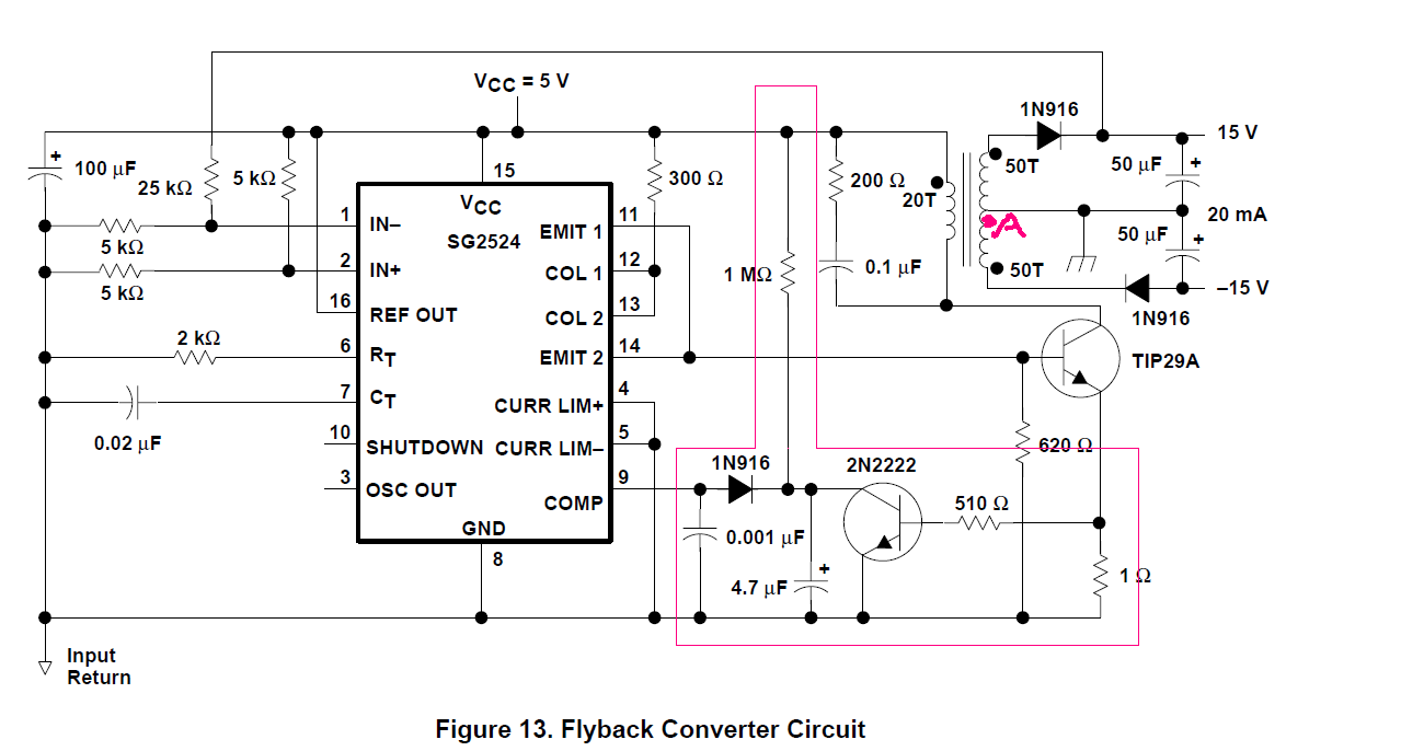
我对这个图有几个疑惑
1.次级输出电压反馈回sg3524没有用光耦,而是直接将输出用电阻网络直接反馈回IN-。这样做是不是初级次级应该把俩个地共起来,(否则反馈了个悬空信号而已)
但是TI的里面俩个地明显画的是俩个不同的啊。。?
2.对于COMP引脚那边连出来的电路(红框部分)不了解,希望能得到详细点的解答
3.我分析了下这个电路结构,觉得下面那个副边线圈(-15V对应那个) 对应的同名端应该是 中间那个节点A而不是它标的那个,请问我的理解是否正确
我对这个图有几个疑惑
1.次级输出电压反馈回sg3524没有用光耦,而是直接将输出用电阻网络直接反馈回IN-。这样做是不是初级次级应该把俩个地共起来,(否则反馈了个悬空信号而已)
但是TI的里面俩个地明显画的是俩个不同的啊。。?
2.对于COMP引脚那边连出来的电路(红框部分)不了解,希望能得到详细点的解答
3.我分析了下这个电路结构,觉得下面那个副边线圈(-15V对应那个) 对应的同名端应该是 中间那个节点A而不是它标的那个,请问我的理解是否正确
