Other Parts Discussed in Thread: BQ79616

This thread has been locked.
If you have a related question, please click the "Ask a related question" button in the top right corner. The newly created question will be automatically linked to this question.

您好
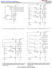
1,根据手册上描述应该是按照a连接。
It is recommended to populate the battery cells from bottom channels (both VC and CB channels) and up,
leaving upper channels as unused channels if cell module size is smaller than the maximum channel size of the
BQ7961x-Q1 device.
2,3 正在询问更了解这款芯片TI 工程师,稍后回复。
您好,请参考下面内容。
The temperature measurement is intended to be done ratiometrically to make sensing more accurate. The temperature can be approximated by testing what is the voltage drop across the NTC. To do this it is recommended to have a pull-up resistor to TSREF that is equal to the NTC resistance at nominal temperature, then the NTC at the GPIO pin. You could optionally add a low-pass filter to mitigate high-frequency noise. Trying to use the GPIO pins differentially would not work since all GPIO pins are programmed to be floating inputs with a weak pulldown resistor.
As for the bus bar resistor, how are you connecting the busbar? Through the BBP/BBN pins or through the VC channels?
您好,So the BQ79616 does not do current measurement through the busbar pins. The BQ7965x family of devices (BQ79656, BQ79654, and BQ79652) does have the current sense capability with a shunt resistor. For these devices, the shunt resistor value should be chosen based on the maximum current and the absolute max voltage range (R_shunt*Imax<Vcs_max) as well as the maximum normal current and the recommended Vcs range (R_shunt*I_typical<Vcs_typical_max). Higher suitable resistance values lead to better ADC resolution but result in higher inefficiency, so that tradeoff would have to be made by the engineer(s).