

Other Parts Discussed in Thread: BQ500212A, INA199
最近有无线充电器项目需要用到bq500212这个芯片,现在以下几个问题请教TI的工程师:
1、按照官网的设计参考的理图设计是否可以通过CE和FCC测试? 在Layout的时候需要注意哪些问题?
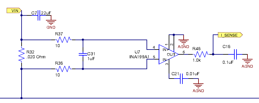
2、官网的设计参考原理图中的U7用的是TI的INA199A1,根据INA199A1的规格书上描述2脚是GND,3脚是VDD;bq500212A的设计参考原理图把INA199A1的2脚和3脚都接到了AGND,这里是不是有问题?若有问题,INA199A1的3脚需要接到哪里?5V_VCC还是3.3V_VCC ?
3、官网的设计参考文件
