Other Parts Discussed in Thread: BQSTUDIO
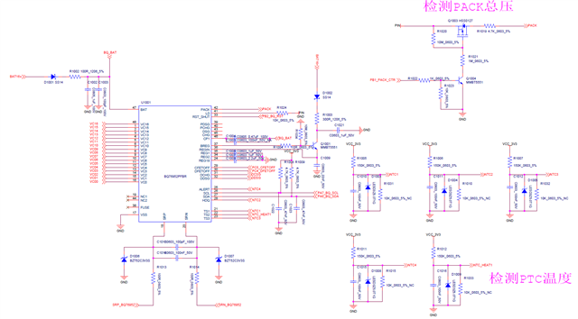
用芯片的DCHG和DDSG管脚驱动外部第三方DRIVER使能MOS,此时偶发AFE芯片不输出DCHG和DDSG高电平5V信号,经过排查,是因为我们在芯片的LD管脚接了10K上拉电阻到PACK+,导致芯片偶发出现此故障,去掉电阻后,可以正常输出5V
This thread has been locked.
If you have a related question, please click the "Ask a related question" button in the top right corner. The newly created question will be automatically linked to this question.
您好,请参考下面内容
The current schematic set-up should be okay but what I am unclear of is if the DDSG and DCHG pins are configured correctly. Could you please send device register settings or preferably the .gg file to verify ?
As for the LD pin there are some considerations to be taken for low-side FET drive. The following application note: https://www.ti.com/lit/ml/sluaa84a/sluaa84a.pdf Section 7 Controlling LD may provide some insight. It is mentioned that the LD pin can have a series resistance between it and Pack+ or it can also go to directly to VSS with some caveats further described in the app note. I am unsure if the LD pin can be left floating but I can follow up on this next.

gg文件需要连接BQstudio生成?这个文件我们不懂怎么生成,可以看下代码配置
#include "include.h"
extern I2C_HandleTypeDef hi2c3;
extern IWDG_HandleTypeDef hiwdg;
#define DEV_ADDR 0x10 // BQ769x2 address is 0x10 including R/W bit or 0x8 as 7-bit address
#define R 0 // Read; Used in DirectCommands and Subcommands functions
#define W 1 // Write; Used in DirectCommands and Subcommands functions
typedef enum
{
Control_Status = 0,
Alert_A = 0x2, //报警状态
Faults_A =0x3, //故障状态
Alert_B = 0x4,
Faults_B =0x5,
Alert_C= 0x6,
Faults_C =0x7,
SLEEP_MODE =0xF,
Battery_Status = 0x12, //电池状态
CHGTEST = 0x001f,
DSGTEST = 0x0020,
FET_EN = 0x0022,
PF_ENABLE = 0x0024,
PF_CLEAR = 0x0029,
PACK_Voltage = 0x36, //总压
CC2_Current = 0x3A, //电流
MANUFACTURINGSTATUS = 0x0057, //工厂模式状态寄存器
Alarm_Status = 0x62, //报警状态
Alarm_Enable = 0x66, //报警使能
DFETOFFTemperature=0x6c,
TS1 = 0x70, //TS1 温度
TS2 = 0x72, //TS2 温度
TS3 = 0x74, //TS3 温度
DASTATUS5 = 0x75,
FET_Status = 0x7F,
CB_ACTIVE_CELLS=0X83,
ShutDown = 0x0010,
SET_CFGUPDATE = 0x0090,
EXIT_CFGUPDATE = 0x0092,
DSG_PDSG_OFF = 0x0093,
CHG_PCHG_OFF = 0x0094,
ALL_FETS_OFF = 0X0095,
ALL_FETS_ON = 0x0096,
FET_CONTROL = 0x0097,
SLEEP_ENABLE = 0x0099,
SLEEP_DISABLE = 0x009A,
PowerConfig = 0x9234 , //Settings:Configuration:Power Config
REG12Config = 0x9236 , //Settings:Configuration:REG12 Config
REG0Config = 0x9237 , //Settings:Configuration:REG0 Config
CommType = 0x9239, //IIC 速率配置
Protection = 0x925F,
EN_Protection_A = 0x9261,
EN_Protection_B = 0x9262,
EN_Protection_C = 0x9263,
CHG_FET_A = 0x9265,
CHG_FET_B = 0x9266,
CHG_FET_C = 0x9267,
DSG_FET_A = 0x9269,
DSG_FET_B = 0x926A,
DSG_FET_C = 0x926B,
CUV = 0x9275, //欠压
CUV_Delay = 0x9276,
COV = 0x9278, //过压
COV_Delay = 0x9279, //过压保护延时
CUV_Recovery = 0x927B,
COV_Recovery = 0x927c , //过压恢复
OCC = 0x9280, //充电过流
OCC_Delay = 0x9281, //充过流保护延时
OCD1=0x9282,
OCD1_Delay=0x9283,
OCD2 = 0x9284, //放电过流
OCD2_Delay = 0x9285, //放电过流保护延时
SCD = 0x9286, //短路
SCD_Delay = 0x9287, //短路延时
SCD_Delay_R=0x9294,
OCD3 = 0x928A, //放电过流
OCD3_Delay = 0x928C, //放电过流保护延时
OCC_Recovery = 0x9288, //充过流恢复
OCD_Recovery = 0x928d, //放电过流恢复
OTC= 0x929A, //overtemperature in Charge
OTC_Delay = 0x929b,
OTC_Recovery = 0x929c,
OTD = 0x929D,
OTD_Delay = 0x929e,
OTD_Recovery = 0x929f,
OTF = 0x92A0, //mos 过温
OTF_Delay = 0x92a1,
OTF_Recovery = 0x92a2,
OTINT = 0x92a3, // Internal Overtemperature
OTINT_Delay = 0x92a4,
OTINT_Recovery = 0x92a5,
UTC = 0x92A6,
UTC_Delay = 0x92a7,
UTC_Recovery =0x92a8,
UTD = 0x92A9,
UTD_Delay = 0x92aa,
UTD_Recovery = 0x92ab,
UTINT = 0x92AC,
UTINT_Delay = 0x92ad,
UTINT_Recovery = 0x92ae,
Recovery = 0x92af, //配置多个保护恢复时间
HWMX = 0x92F9,
CFETOFFPinConfig = 0x92FA ,
DFETOFFPinConfig = 0x92FB , //Settings:Configuration:DFETOFF Pin Config
ALERTPinConfig=0x92FC,
HQDPinConfig=0x9300,
TS1Config = 0x92FD , //Settings:Configuration:TS1 Config
TS2Config = 0x92FE , //Settings:Configuration:TS2 Config
TS3Config = 0x92FF , //Settings:Configuration:TS3 Config
HDQTemperature = 0x76 ,
ALERTTemperature = 0x6E,
DDSGTemperature = 0x7A,
DCHGPinConfig = 0x9301,
DDSGPinConfig = 0x9302,
DA = 0x9303, //可以配置用户电压、电流单位精度
Vcell = 0x9304,
CC3_samples = 0x9307,//The device provides an averaged current reading (CC3) over a configurable number of CC2 Current samples
FET_Options = 0x9308 , //Settings :FET
Chg_Pump_Control = 0x9309,
BalancingConfig=0x9335,
Mfg_Status = 0x9343,
}FW_AFE_Command;
static BMS_ARGCFG *FW_bms_ArgCfg;
static unsigned short balanceFlag=0;
static unsigned char Balance_Addr[4]={0};
static unsigned short fw_afe_vol[16]={0};//用于内部均衡
static void I2C_WriteReg(unsigned char reg_addr, unsigned char *reg_data, unsigned char count)
{
HAL_I2C_Mem_Write(&hi2c3, DEV_ADDR, reg_addr, 1, reg_data, count, 1000);
}
static unsigned char I2C_ReadReg(unsigned char reg_addr, unsigned char *reg_data, unsigned char count)
{
HAL_I2C_Mem_Read(&hi2c3, DEV_ADDR, reg_addr, 1, reg_data, count, 1000);
return 1;
}
/*
**校验和
*/
static unsigned char Checksum(unsigned char *ptr, unsigned char len)
// Calculates the checksum when writing to a RAM register. The checksum is the inverse of the sum of the bytes.
{
unsigned char i;
unsigned char checksum = 0;
for(i=0; i<len; i++)
checksum += ptr[i];
checksum = 0xff & ~checksum;
return(checksum);
}
/*
**直接命令写
*/
/*static void DirectCommands_Write(unsigned char command, unsigned short data)
{
unsigned char TX_data[2]={0};
//little endian format
TX_data[0] = data & 0xff;
TX_data[1] = (data >> 8) & 0xff;
I2C_WriteReg(command,TX_data,2); //Control_status, alarm_status, alarm_enable all 2 bytes long
HAL_Delay(1);
}*/
/*
**直接命令读
*/
static void DirectCommands_Read(unsigned char command,unsigned char *buff,unsigned char n)
{
I2C_ReadReg(command, buff, n); //RX_data is a global variable
HAL_Delay(1);
}
/*
**子命令
*/
static void CommandSubcommands(unsigned short command) //For Command only Subcommands
// See the TRM or the BQ76952 header file for a full list of Command-only subcommands
{ //For DEEPSLEEP/SHUTDOWN subcommand you will need to call this function twice consecutively
unsigned char TX_Reg[2] = {0x00, 0x00};
//TX_Reg in little endian format
TX_Reg[0] = command & 0xff;
TX_Reg[1] = (command >> 8) & 0xff;
I2C_WriteReg(0x3E,TX_Reg,2);
HAL_Delay(60);
}
/*
**子命令读寄存器
*/
static void DataRAM_Read(unsigned short addr, unsigned char *buff, unsigned char length)
{
unsigned char addressBlock[2] = {0};
/*
Write address location to 0x3E and read back from 0x40
Used to read configuration registers and for subcommands
*/
addressBlock[0] = addr%256;
addressBlock[1] = (addr/256);
I2C_WriteReg(0x3E,addressBlock,2);
I2C_ReadReg(0x40, buff,length);
}
/*
**子命令写寄存器
*/
void DataRAM_Write(unsigned short addr,unsigned char block)
{
unsigned char addressBlock[2] = {0};
unsigned char wholeBlock[2] = {0};
unsigned char data[2] = {0};
/*
Write address location to 0x3E and Checksum,length to 0x60
Used to write configuration registers
*/
addressBlock[0] = addr%256;
addressBlock[1] = (addr/256);
wholeBlock[0] = addressBlock[0] + block;
wholeBlock[1] = addressBlock[1] + block;
data[0] = ~(wholeBlock[0]+wholeBlock[1]) & 0xff;
data[1] = strlen((char *)wholeBlock)+2;
I2C_WriteReg(0x3E,wholeBlock,2);
I2C_WriteReg(0x60, data, 2);
}
/*
**寄存器设置
*/
void BQ769x2_SetRegister(unsigned short reg_addr, unsigned long reg_data, unsigned short datalen)
{
unsigned char TX_Buffer[2] = {0x00, 0x00};
unsigned char TX_RegData[6] = {0x00, 0x00, 0x00, 0x00, 0x00, 0x00};
//TX_RegData in little endian format
TX_RegData[0] = reg_addr & 0xff;
TX_RegData[1] = (reg_addr >> 8) & 0xff;
TX_RegData[2] = reg_data & 0xff; // 1st byte of data
switch(datalen)
{
case 1:// 1 byte datalength
I2C_WriteReg(0x3E, TX_RegData, 3);
HAL_Delay(2);
TX_Buffer[0] = Checksum(TX_RegData, 3);
TX_Buffer[1] = 0x05; //combined length of register address and data
I2C_WriteReg(0x60, TX_Buffer, 2); // Write the checksum and length
HAL_Delay(2);
break;
case 2: // 2 byte datalength
TX_RegData[3] = (reg_data >> 8) & 0xff;
I2C_WriteReg(0x3E, TX_RegData, 4);
HAL_Delay(2);
TX_Buffer[0] = Checksum(TX_RegData, 4);
TX_Buffer[1] = 0x06; //combined length of register address and data
I2C_WriteReg(0x60, TX_Buffer, 2); // Write the checksum and length
HAL_Delay(2);
break;
case 4: // 4 byte datalength, Only used for CCGain and Capacity Gain
TX_RegData[3] = (reg_data >> 8) & 0xff;
TX_RegData[4] = (reg_data >> 16) & 0xff;
TX_RegData[5] = (reg_data >> 24) & 0xff;
I2C_WriteReg(0x3E, TX_RegData, 6);
HAL_Delay(2);
TX_Buffer[0] = Checksum(TX_RegData, 6);
TX_Buffer[1] = 0x08; //combined length of register address and data
I2C_WriteReg(0x60, TX_Buffer, 2); // Write the checksum and length
HAL_Delay(2);
break;
}
}
/*
**初始化
*/
void AFE_Init(void)
{
HAL_GPIO_WritePin(BQ_RST_GPIO_Port,BQ_RST_Pin, GPIO_PIN_SET); // RST_SHUT pin set low
HAL_IWDG_Refresh(&hiwdg);
HAL_Delay(1000);
HAL_GPIO_WritePin(BQ_RST_GPIO_Port,BQ_RST_Pin, GPIO_PIN_RESET);
}
/*
**唤醒
*/
void AFE_WakeUp(void)
{
unsigned char times=0;
unsigned char value=0;
AFE_Init();
while(value!= 1)
{
HAL_IWDG_Refresh(&hiwdg);
DirectCommands_Read(0,&value,1);
HAL_Delay(10);
HAL_GPIO_WritePin(BQ_WK_GPIO_Port, BQ_WK_Pin,GPIO_PIN_SET);
HAL_Delay(200);
HAL_GPIO_WritePin(BQ_WK_GPIO_Port, BQ_WK_Pin,GPIO_PIN_RESET);
times++;
if(times > 1)
{
break;
}
}
}
/*
**过压配置
*/
void AFE_COV_Configuration(void)
{
BQ769x2_SetRegister(COV,((FW_bms_ArgCfg->C_S_V_H+50)*10)/506,1);
HAL_Delay(1);
BQ769x2_SetRegister(COV_Delay,(FW_bms_ArgCfg->C_S_V_H_Delay*10-66)/33,2);
HAL_Delay(1);
BQ769x2_SetRegister(COV_Recovery,(((FW_bms_ArgCfg->C_S_V_H)-(FW_bms_ArgCfg->C_S_V_H_R_V)-50)*10)/506,1);
HAL_Delay(1);
}
/*
**欠压配置
*/
void AFE_CUV_Configuration(void)
{
BQ769x2_SetRegister(CUV,(FW_bms_ArgCfg->D_S_V_L-50)*10/506,1);
HAL_Delay(1);
BQ769x2_SetRegister(CUV_Delay,(FW_bms_ArgCfg->D_S_V_L_Delay*10-66)/33,2);
HAL_Delay(1);
BQ769x2_SetRegister(CUV_Recovery,((FW_bms_ArgCfg->D_S_V_L_R_V)-(FW_bms_ArgCfg->D_S_V_L)+50)*10/506,1);
HAL_Delay(1);
}
/*
**充电过流配置
*/
void AFE_OCC_Configuration(void)
{
short OCC_Recovery_Value=1000;
BQ769x2_SetRegister(OCC,(unsigned long )(FW_bms_ArgCfg->C_C_H_1*FW_bms_ArgCfg->CurSample)/100/200,1);
HAL_Delay(1);
BQ769x2_SetRegister(OCC_Delay,(FW_bms_ArgCfg->C_C_H_1_Delay*10-66)/33,1);
HAL_Delay(1);
BQ769x2_SetRegister(OCC_Recovery,OCC_Recovery_Value,2);
HAL_Delay(1);
}
/*
**放电过流配置
*/
void AFE_OCD_Configuration(void)
{
short OCD_Recovery_Value=1000;
BQ769x2_SetRegister(OCD1,(unsigned long )(FW_bms_ArgCfg->D_C_H_1*FW_bms_ArgCfg->CurSample)/100/200,1);
HAL_Delay(1);
BQ769x2_SetRegister(OCD1_Delay,(FW_bms_ArgCfg->D_C_H_1_Delay*10-66)/33,1);
HAL_Delay(1);
BQ769x2_SetRegister(OCD2,(unsigned long )(FW_bms_ArgCfg->D_C_H_2*FW_bms_ArgCfg->CurSample)/100/200,1);
HAL_Delay(1);
BQ769x2_SetRegister(OCD2_Delay,(FW_bms_ArgCfg->D_C_H_2_Delay*10-66)/33,1);
HAL_Delay(1);
BQ769x2_SetRegister(OCD3,(0-(unsigned long )(FW_bms_ArgCfg->D_C_H_3*FW_bms_ArgCfg->CurSample)/100),2);
HAL_Delay(1);
BQ769x2_SetRegister(OCD3_Delay,FW_bms_ArgCfg->D_C_H_3_Delay/1000,1);
HAL_Delay(1);
BQ769x2_SetRegister(OCD_Recovery,0-OCD_Recovery_Value,2);
HAL_Delay(1);
}
/*
**短路、过流保护延时配置
*/
void AFE_SCD_OCD_Configuration(void)
{
BQ769x2_SetRegister(SCD,FW_bms_ArgCfg->D_S_C,1);
HAL_Delay(1);
BQ769x2_SetRegister(SCD_Delay,FW_bms_ArgCfg->D_S_C_Delay+1,1);
HAL_Delay(1);
BQ769x2_SetRegister(SCD_Delay_R,FW_bms_ArgCfg->D_S_C_R_Delay,1);
}
/*
**CHGFET and DSGFET 保护功能启用配置
*/
void AFE_CHGFET_DSGFET_Function_Configuration(void)
{
BQ769x2_SetRegister(CHG_FET_A,0X18,1);//0X98
HAL_Delay(1);
BQ769x2_SetRegister(CHG_FET_B,0,1); // 所有温度报警不进行保护
HAL_Delay(1);
BQ769x2_SetRegister(CHG_FET_C,0X1,1);//
HAL_Delay(1);
BQ769x2_SetRegister(DSG_FET_A,0XE4,1);//0XE4
HAL_Delay(1);
BQ769x2_SetRegister(DSG_FET_B,0,1);// 所欲温度报警不进行保护
HAL_Delay(1);
BQ769x2_SetRegister(DSG_FET_C,0X80,1);
HAL_Delay(1);
}
/*
**温度通道采集配置
*/
void AFE_TS_Configuration(void)
{
BQ769x2_SetRegister(TS1Config,0xB3,1);// 电池温度1
HAL_Delay(1);
BQ769x2_SetRegister(TS2Config,0xb3,1);//配置此温度为只采集不保护,因为此温度为加热膜温度
HAL_Delay(1);
BQ769x2_SetRegister(TS3Config,0xB3,1);//电池温度2
HAL_Delay(1);
BQ769x2_SetRegister(HQDPinConfig,0XB3,1);//电池温度3
HAL_Delay(1);
BQ769x2_SetRegister(ALERTPinConfig,0Xb3,1);//电池温度4
HAL_Delay(1);
}
/*
**DFET and CFET pin脚功能配置
*/
void AFE_DFET_CFET_Configuration(void)
{
BQ769x2_SetRegister(DFETOFFPinConfig,0x82,1);//配置为ADC输入了
HAL_Delay(1);
BQ769x2_SetRegister(CFETOFFPinConfig,0x82,1);//配置为正常输出
HAL_Delay(1);
}
/*
**保护功能启用配置
*/
void AFE_Protection_Configuration(void)
{
BQ769x2_SetRegister(EN_Protection_A,0xfc,1);//0xfc
HAL_Delay(1);
BQ769x2_SetRegister(EN_Protection_B,0x0,1);
HAL_Delay(1);
BQ769x2_SetRegister(EN_Protection_C,0x80,1);//0x80
HAL_Delay(1);
}
/*
**工厂模式、FET功能启用等其他配置
*/
void AFE_Mode_Function_Configuration(void)
{
BQ769x2_SetRegister(DA,6,1);//总压采集精度为10mV 电流采集精度为10mA
HAL_Delay(1);
BQ769x2_SetRegister(Vcell,FW_bms_ArgCfg->BatUseFlag,2);
HAL_Delay(1);
BQ769x2_SetRegister(Protection,0,2);//不启用短路保护SCDL恢复、永久故障保护
HAL_Delay(1);
BQ769x2_SetRegister(Mfg_Status,0x10,1);//设置FET_en
HAL_Delay(1);
BQ769x2_SetRegister(FET_Options,0xf,1);
HAL_Delay(1);
CommandSubcommands(SLEEP_DISABLE);
HAL_Delay(1);
BQ769x2_SetRegister(Chg_Pump_Control,1,1);
HAL_Delay(1);
BQ769x2_SetRegister(CommType,8,1);
HAL_Delay(1);
}
/*
**供电电源配置
*/
void AFE_Power_Configuration(void)
{
BQ769x2_SetRegister(PowerConfig,0x2D80,2);
HAL_Delay(1);
BQ769x2_SetRegister(REG0Config,0x1,1);
HAL_Delay(1);
BQ769x2_SetRegister(REG12Config,0xFF,1); //配置内部REG1 和REG2都是5V
HAL_Delay(1);
}
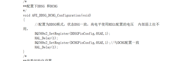
/*
**配置下DDSG 和DCHG
*/
void AFE_DDSG_DCHG_Configuration(void)
{
//配置为DDSG模式,状态DSG一致,高电平使用REG1配置的电压 内部弱上拉不用,
BQ769x2_SetRegister(DDSGPinConfig,0XAE,1);
HAL_Delay(1);
BQ769x2_SetRegister(DCHGPinConfig,0XAE,1);//与DCHG配置一致
HAL_Delay(1);
}
/*
**参数初始化设置
*/
void AFE_ArgCfg_Set(BMS_ARGCFG bms_ArgCfg)
{
FW_bms_ArgCfg=&bms_ArgCfg;
CommandSubcommands(SET_CFGUPDATE);// 进入配置模式
//COV 配置
AFE_COV_Configuration();
//CUV 配置
AFE_CUV_Configuration();
//OCC 配置
AFE_OCC_Configuration();
//OCD配置
AFE_OCD_Configuration();
//电源配置
AFE_Power_Configuration();
//温度通道采集配置
AFE_TS_Configuration();
//DFET and CFET pin脚功能配置
AFE_DFET_CFET_Configuration();
HAL_IWDG_Refresh(&hiwdg);
//保护功能启用配置
AFE_Protection_Configuration ();
//工厂模式、FET功能启用等其他配置
AFE_Mode_Function_Configuration();
//CHGFET and DSGFET 保护功能启用配置
AFE_CHGFET_DSGFET_Function_Configuration();
//短路、过流保护延时配置
AFE_SCD_OCD_Configuration();
//配置DDSG和DCHG
AFE_DDSG_DCHG_Configuration();
//整个系统的延时回复
BQ769x2_SetRegister(Recovery,5,1);
//开启均衡
BQ769x2_SetRegister(BalancingConfig,0xf,1);
// Exit CONFIGUPDATE mode - Subcommand 0x0092
BQ769x2_SetRegister(CC3_samples, 80, 1);
//设置CC3为CC2平均值的采样个数
CommandSubcommands(EXIT_CFGUPDATE);
HAL_IWDG_Refresh(&hiwdg);
//将BQ先配置位关,因为此时12V没有起来 ,驱动用的12V是跟外部供电12V
HAL_Delay(500);
AFE_MosControl_Set(0);
}
/*
**读取AD值
*/
unsigned short AFE_Cell_Temp_Read_AD(unsigned char command)
{
unsigned char Inter_buff[2]={0};
unsigned short buff=0;
DirectCommands_Read(command,Inter_buff,2);
buff=Inter_buff[1]*256+Inter_buff[0];
return buff;
}
/*
**读子命令
*/
void CommandSubcommands_Read(unsigned short command)
{
CommandSubcommands(command);
HAL_Delay(1);
I2C_ReadReg(0x40,NULL,2);
}
int mian()
{
AFE_WakeUp();
AFE_ArgCfg_Set(bms_ArgCfg);
unsigned short Vol[16]={0};
AFE_Cell_Vol_Read(Vol);
}
您好,请参考下面内容:
The settings you sent look good to me, I cant really explain why you are seeing this behavior when you have the 10kOhm resistor vs without it on the LD pin. I have verified that if the LD pin is left floating in the case of low-side FET drive (DSG and CHG FET drivers not used) this should be okay but in general we think that tying it to VSS would be safer.
On another note, on the schematic we do recommend you use capacitors to ground instead of zener diodes or Schottky diode if you prefer this on the SRP/SRN pins. This is because the zener may affect your voltage measurement. You may also see this E2E discussion where it is discussed further in the thread:https://e2e.ti.com/support/power-management-group/power-management/f/power-management-forum/1080696/bq76952-bq7695202