

您好,
為何BQ76952 REG1V8 引腳上的電壓在與MCU通訊後會被拉到3.3V
線路架構在 CFETOFF, DFETOFF, 有一外部上拉電阻到3.3V
Settings:Configuration:CFETOFF Pin Config 設置為 AA
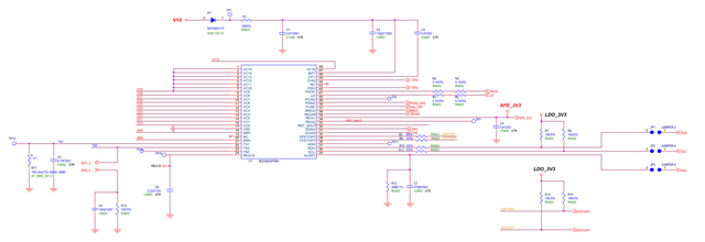
电路如貼圖
Original question:

您好,
為何BQ76952 REG1V8 引腳上的電壓在與MCU通訊後會被拉到3.3V
線路架構在 CFETOFF, DFETOFF, 有一外部上拉電阻到3.3V
Settings:Configuration:CFETOFF Pin Config 設置為 AA
电路如貼圖
