If you have a related question, please click the "Ask a related question" button in the top right corner. The newly created question will be automatically linked to this question.
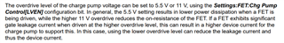
您好,The BQ76952 uses the charge pump to drive the CHG and DSG FETs. The charge pump will use an overdrive voltage which can be set to 11V or 5.5V. By default this is set to 11V.
Basically the Vgs voltage is either 5.5V or 11V. This is also explained in Section 5.2.2 High-Side NFET Drivers of the Technical Reference Manual
Note: Whenever the charge pump is in operation (in 5.5 V or 11 V mode), the maximum voltage on VBAT should be reduced to ensure the voltage on CP1, CHG, and DSG does not exceed their maximum specified voltage.