If you have a related question, please click the "Ask a related question" button in the top right corner. The newly created question will be automatically linked to this question.
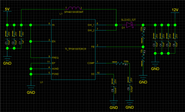
TPS61087: When the output current increases slightly from 5V to 12V, the output voltage will decrease and cannot reach the 900mA output current described in the data manual