If you have a related question, please click the "Ask a related question" button in the top right corner. The newly created question will be automatically linked to this question.
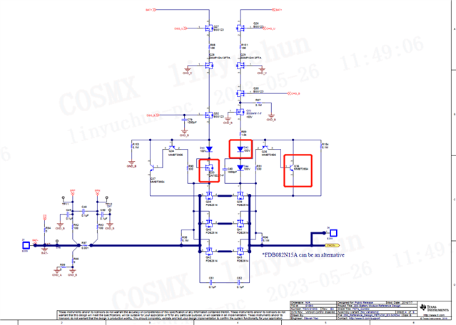
1- R3 and C3 are part of the recommended filter components for the supply pins. See below for D6. More info can be found in this video
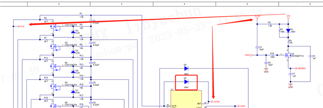
2- The purpose of Q33 is to add a voltage drop along with D41 to lower the voltage at the gates of Q38, Q40, and Q42 (this is explained in the Design guide). I would assume D42 is for the same purpose, to lower the gate voltage for Q39, Q41, Q43.
3, The purpose of Q36 is to expedite to extract and exhaust the charges on the gate of Q39 so that the cut off speed of Q39 can be desired for actual application, adjusting the value of R91 can change the FET cut off speed.
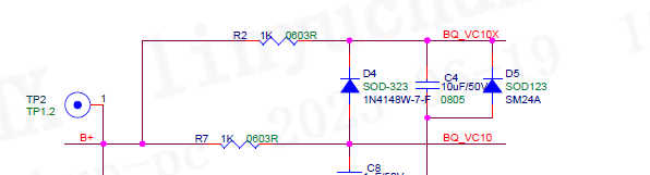
1, D6 is a flyback diode as described in page 27 of the EVM user guide www.ti.com/.../slvu924d.pdf If the discharge FET turns off quickly with high current and with a large inductive load on the pack terminals, the inductance may create a high voltage on the PACK- terminal. D6 will limit the voltage to near the PACK- terminal. D6 may not be needed, without D6 the discharge FET may handle such a voltage surge with its avalanche rating. While the bq76920 has a non-zero pull down resistance which will avoid an instant turn off of the discharge FET, the EVM has the R16 resistor to the gate as 0. Resistance can be added at the R16 location to slow switching to avoid the fast dI/dt which can cause the transient. The designer should select a turn off which will not cause the FET to overheat during switching.
D6 will be forward biased when the discharge FET is turned off as the current would continue to flow from Pack- to Pack+ via D6, since it is forward biased, the Pack- voltage is clamped to Pack+, this is how Pack- voltage is limited.
I haven't tried with direct connecting Pin3 of Q35 to GND, suggest to make a simulation to check the result
D6 will be forward biased when the discharge FET is turned off as the current would continue to flow from Pack- to Pack+ via D6, since it is forward biased, the Pack- voltage is clamped to Pack+, this is how Pack- voltage is limited.
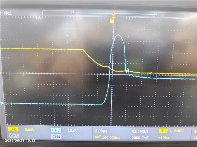
i did a short test, the BMS with D6, but the P- voltage was not clamped to BAT(i think it should be BAT instead of PACK+). the volatage of P- is double than BAT. could you tell me why?
您好, Do you have the plot of short test, in the schematic of P29, Pack- shall be clamped to BATT+ when the discharge path is cut off, due to respond delay of D6, a brief high pulse on PACK- may be observed, but it should be quickly clamped by D6, D6 should be selected with appropriate forward clamping respond speed so that the brief pulse won't damage other components in the circuit.
您好, Do you have the plot of short test, in the schematic of P29, Pack- shall be clamped to BATT+ when the discharge path is cut off, due to respond delay of D6, a brief high pulse on PACK- may be observed, but it should be quickly clamped by D6, D6 should be selected with appropriate forward clamping respond speed so that the brief pulse won't damage other components in the circuit.