(1) In the datasheet, there is a description: it can operate with an input supply voltage as low as 1.5V if the BIAS pin is greater than 2.9V. I don't know the reason and the logic of this sentence. How does the BIAS Pin voltage influence the minimum supply voltage? As I known, the BIAS Pin usually connects to V(supply) directly in fly-back. in this condition, the V(BIAS) is equal to V(supply).
(2) There is a diode connected between BIAS and VCC regulator’s output, what is the uses of this diode?
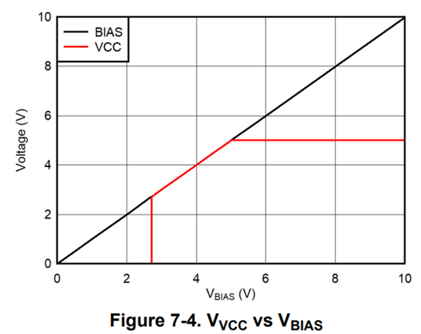
This is my assumption: When the V(BIAS) less than 5V, the diode is forward and the output voltage of the VCC regulator is equal to V(BIAS). I guess this can explain the curves shown in datasheet (see Fig7-4 in datasheet) However, there is another question: why the VCC regular voltage change with V(BIAS) but not be a constant value (5 V) when the VBIAS below 5V? Will the low voltage (below 5V) influence its driven capability for internal MOSFET?