

Part Number: TPS65930
1.Environment settings
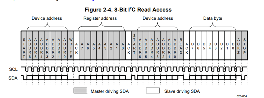
The chip IIC mode is Slave mode (SC021 mode, BOOT0=1, BOOT1=1), and the test machine (or IIC protocol debugger) is the master, and the corresponding format of the power address and the IIC address is as follows,
|
ID1 Read IIC [0x48=01001000]<-> IIC Read Adress 10010001=0x91 |
|
ID1 Write IIC [0x48=01001000]<-> IIC Write Adress 10010000=0x90 |
|
ID2 Read IIC [0x49=01001001]<-> IIC Read Adress 10010011=0x93 |
|
ID2 Write IIC [0x49=01001001]<-> IIC Write Adress 10010010=0x92 |
|
ID3 Read IIC [0x4a=01001010]<-> IIC Read Adress 10010101=0x95 |
|
ID3 Write IIC [0x4a=01001010]<-> IIC Write Adress 10010100=0x94 |
|
ID4 Read IIC [0x4B=01001011]<-> IIC Read Adress 10010111=0x97 |
|
ID4 Write IIC [0x4B=01001011]<-> IIC Write Adress 10010110=0x96 |
|
ID5 Read IIC [0x12=00010010]<-> IIC Read Adress 00100101=0x25 |
|
ID5 Write IIC [0x12=00010010]<-> IIC Write Adress 00100100=0x24 |
When testing IIC communication, VDD1 output is 1.0V, VDD2 output is 1.1V, VIO output is 1.76V, and VPPL1 output is 1.8V
2.Test instructions
(according to the reference document and our own test have been carried out IIC communication settings and tests, can not be read and written)
1)After power-up, first perform the boot operation, set the PWRON input low, and configure the registers as follows
RegSet(SR-I2C(94H), 04H, 02H ); MCU--1.1V ;
Release PowerOn when the operation is complete
2)Power supply test register configuration
RegSet(SR-I2C(94H), 05H, 00H ) ; MCU--1.2V ;
3)The operation CN_I2C register enable, VAUX2/VMMC/VDAC three LDO outputs
RegSet(CN_I2C(90H), 40H, CBH);
RegSet(CN-I2C(90H), 41H, CBH);
RegSet(CN-I2C(90H), 42H, D9H); MCU--1.3V
All instructions sent in are invalid (address bits, registers have ACK), data bits do not have ACK.
Failed to set the register address and data bits of 40H, 41H, and 42H in the datasheet.
3.What we have already done
We read and write IIC data according to ID4 (0x4B) on the TPS65930 instruction manual, corresponding to the Read, Write addresses of IIC 0x97, 0x96). (P72-P81)
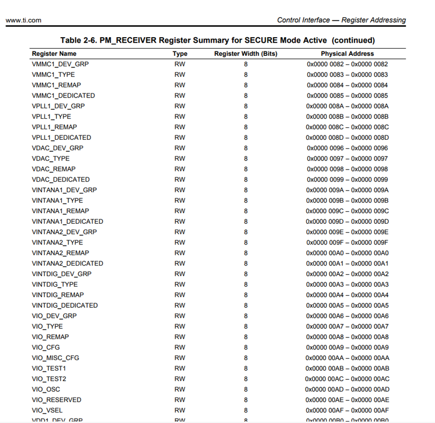
Failed to read VMMC2_DEV_GRP correctly (tried both types of data)
The read VMMC2_DEV_GRP instruction is: 96H 82H 97H.
The read VMMC2_DEV_GRP instruction is: 96H 27H 97H.
Note: (VMMC1_REMAP Address Offset is ·0x27, VMMC1_REMAP Address 0x0000 0082-0x0000 0082, we understand Register Adress as 82H)
I don't know what the problem is, can you guide the correct reading of the instruction data is how much it is? Thank you.
