If you have a related question, please click the "Ask a related question" button in the top right corner. The newly created question will be automatically linked to this question.
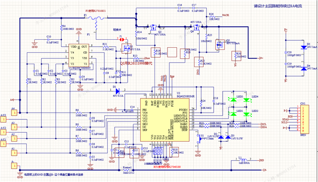
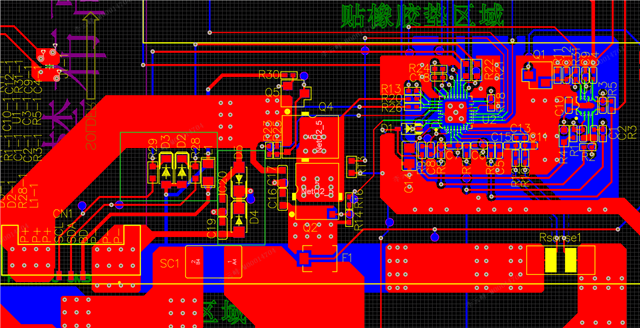
The layout is not ideal, it should have a solid ground plane to help absorb the ESD as much as possible and the caps on PACK+ to PACK- should have as short and thick traces as possible. We see the biggest improvements by adding the ground plane. Also try increasing C19 and C20 to absorb more of the voltage before it is applied to the gauge.