Part Number: LM76003
请问一下
问题一
BIAS 脚位功能是什么呢?
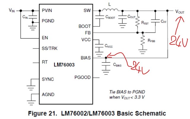
看起来是可以从外部输入电源,让内部的LDO用
这样可以让转换效率提高,请问是吗?
问题二
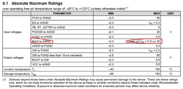
BIAS脚位最高耐压是30V,所以我照公版电路设计
将输出接到BIAS ,是否表示输出电压只能低于30V
问题三
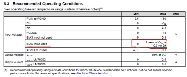
如照公版电路,BIAS脚位需要加上电容Cbias
如果设计输出是24V,当电容Cbias烧毁时
不管是短路或开路,看起来不会造成IC烧毁
请问是吗?
如果因为BIAS脚位短路造成IC烧毁 ,是否表示BIAS有大于30V的电压
才会造成IC烧毁?