This thread has been locked.
If you have a related question, please click the "Ask a related question" button in the top right corner. The newly created question will be automatically linked to this question.
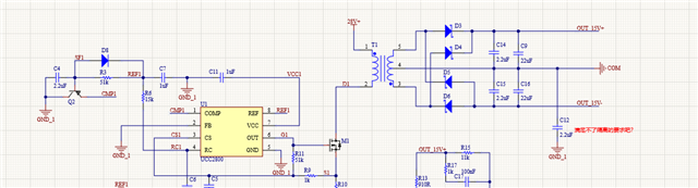
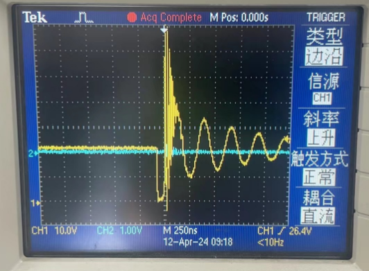
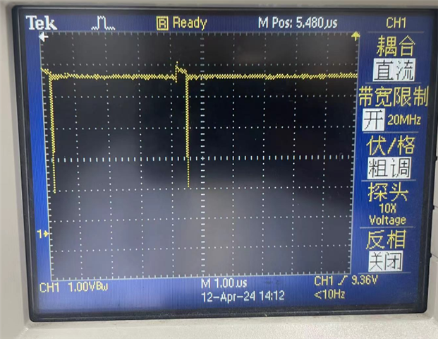
你好,我按原理图方案设计28V输入,±15V输出电压时,测试中发现DRAIN端波形对VCC、REF、CS、RC等引脚信号都形成了干扰,如何去解决呢,是PCB布局的问题吗