

When it comes to MOS tube burnout, it is usually because it is not working in the SOA workspace, and there is also a case where the MOS tube is overcurrent.
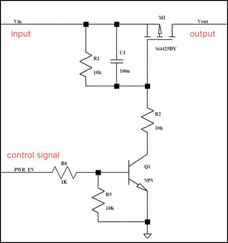
For example, the maximum allowable current of the PMOS transistor in this circuit is 50A, and the maximum current reaches 80+ at the moment when the MOS transistor is turned on, then the current is very large.
At this time, the PMOS is over-specified, and we can see on the SOA curve that it is not working in the SOA range, which will cause the PMOS to be damaged.
So what if you choose a higher current PMOS? Of course you can, but the cost will be higher.
We can choose to adjust the peripheral resistance or capacitor to make the PMOS turn on more slowly, so that the current can be lowered.
For example, when adjusting R1, R2, and the jumper capacitance between gs, when Cgs is adjusted to 1uF, The Ids are only 40A max, which is fine in terms of current, and meets the 80% derating.
(50 A * 0.8 = 40 A).
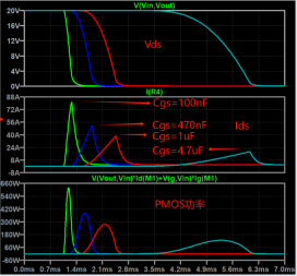
Next, let's look at the power, from the SOA curve, the opening time of the MOS tube is about 1ms, and the maximum power at this time is 280W.
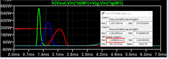
The normal thermal resistance of the chip is 122°F/W, and the maximum junction temperature can be 302°F.
Assuming the ambient temperature is 77°F, then the instantaneous power that 1ms can withstand is about 357W.
The actual power of PMOS here is 280W, which does not exceed the limit, which means that it works normally in the SOA area.
Therefore, when the current impact of the MOS transistor is large at the moment of turning, the Cgs capacitance can be adjusted appropriately to make the PMOS Working in the SOA area, you can avoid the problem of MOS corruption.
