This thread has been locked.
If you have a related question, please click the "Ask a related question" button in the top right corner. The newly created question will be automatically linked to this question.
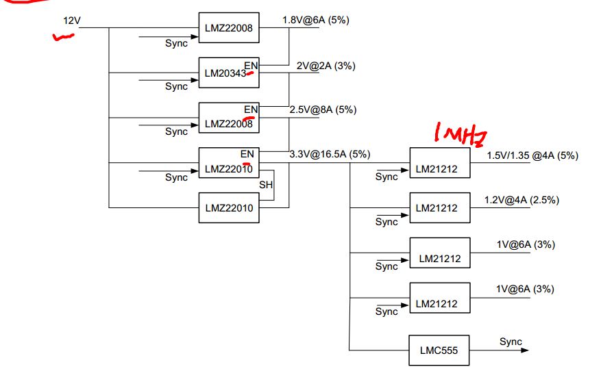
如图示FPGA的TI电源解决方案示例,对于7系列的电源,方案里先产生如3.3V的电压,而后产生1V的电压,是不是与供电顺序——内核到外围的顺序相矛盾,请过来人解答
亲;通常是一个电源过来的;3.3V还没建立;1V已经建立了。


