Although MOS is voltage driven, there is a large junction capacitance between the gate and the source. When it is turned on, a large charging current is required, and when it is turned off, a large discharge current is required. Therefore, a low-impedance charging and discharging path is required.
This is a low-side MOS tube drive circuit. The input end is composed of Q3 and the periphery using a common base connection to form a level
conversion circuit. The control input is received from ⑤, and the control input can be generated by the MCU. The input 3V is converted into an output 12V. Since Q1 Q2 is a complementary emitter follower, there is no problem of Q1 Q2 turning on at the same time to short-circuit the power supply. To prevent accidents, it is a safe practice to connect a resistor in series at the output end.

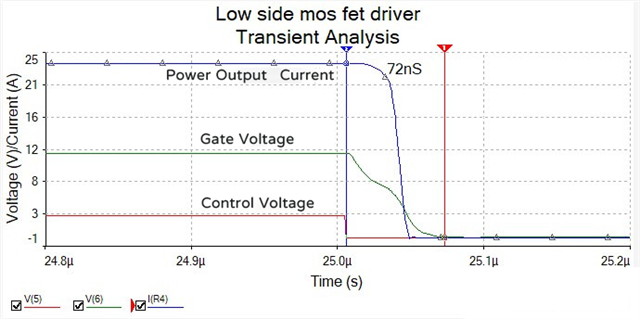
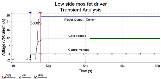
The time required for MOS to turn on from off to on is longer than the time from on to off. Reducing R1 can shorten the time from off to on. But it is not unlimited because the current pulling capacity of the driving source is limited.


When the control voltage changes from low to high, there is a 3V step at the beginning of the gate voltage. Analysis shows that it is caused by the 3.3 bias voltage feeding through the BC junction after Q3 is turned off.
In the switching state, the MOS tube needs to be closed and opened as quickly as possible, and this circuit can effectively control it.
