Part Number: TPS22811
关于TPS22811芯片的问题点如下:
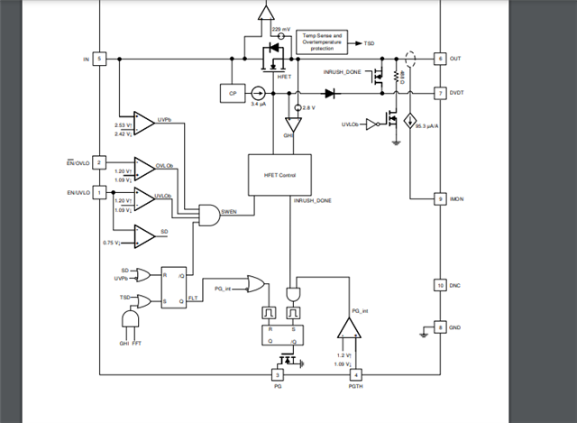
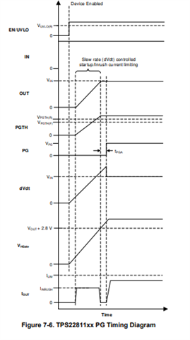
1. 实际应用中,PG和PGTH 具体监控原理是什么?是否为必选?
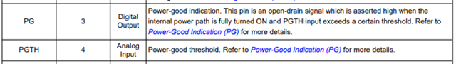
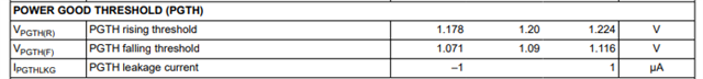
2. PG和PGTH的电压如何正确理解?其中PGTH上升电压(1.2V)是否和UVLO的上升电压(1.2V)原理一致?
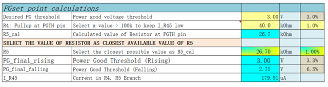
3.如果问题1中,PG和PGTH为必选,如何配合电压进行电阻的匹配?如输出3.3V。
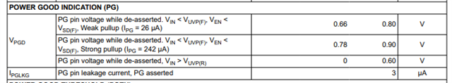
4.正常工作时,PG和PGTH应为高电平,但实际测试评估板均为低电平,但输出电压正常。该现象是否正常?如实际应用中有无影响?
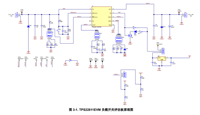
4.1 测试评估板时,欠压和过压电压已配置成功并验证可行,输出电压正常(VIN 3.3V)。PG上拉至VIN(J13 为23连接),PGTH上拉至Vout(J2为12连接)。此时测量PG电压0V,PGTH电压0.35V(1.该0.35V是否可理解为3.3V的电阻分压?理论计算电阻分压为0.35V;2.如为电阻分压,同时更改R12为40K,R13为27K,根据分压PGTH应为1.2V,但实际0V)。