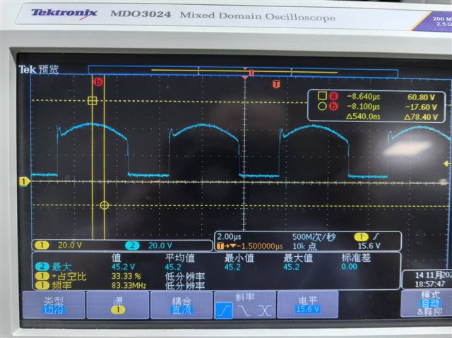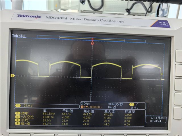

第一个图是重叠时间小的,time引脚电阻30K第二个图是68K,都有一个现象就是VDS的电压波形不对,不知道时哪里设置不对引起的
This thread has been locked.
If you have a related question, please click the "Ask a related question" button in the top right corner. The newly created question will be automatically linked to this question.
您好
LM5026在设计时遇到效率问题,主要表现为随负载增加,效率逐渐降低,且在2-3A负载时效率随器件发热而进一步降低。同时,测试发现开关MOS的Vds波形异常。
建议检查同步整流时序、驱动信号以及变压器,同时考虑优化电路设计和元件选择,以提高效率和解决Vds波形异常问题。
10 Layout 10.1 Layout Guidelines The LM5026 current-sense and PWM comparators are very fast, and respond to short duration noise pulses. The components at the CS, COMP, SS, DCL, UVLO, TIME, SYNC and the RT pins should be as physically close as possible to the IC, thereby minimizing noise pick-up on the PCB tracks. Layout considerations are critical for the current-sense filter. If a current-sense transformer is used, both leads of the transformer secondary should be routed to the sense filter components and to the IC pins. The ground side of each transformer should be connected through a dedicated PCB track to the AGND pin, rather than through the ground plane. If the current-sense circuit employs a sense resistor in the drive transistor source, low inductance resistor should be used. In this case, all the noise-sensitive, low-current ground tracks should be connected in common near the IC, and then a single connection made to the power ground (sense resistor ground point). The gate drive outputs of the LM5026 should have short direct paths to the power MOSFETs in order to minimize inductance in the PCB traces. The two ground pins (AGND, PGND) must be connected together with a short direct connection to avoid jitter due to relative ground bounce. If the internal dissipation of the LM5026 produces high junction temperatures during normal operation, the use of multiple vias under the IC to a ground place can help conduct heat away from the IC. Judicious positioning of the PCB within the end product, along with use of any available air flow (forced or natural convection) can help reduce the junction temperatures.
这是官方的布局指导,您看一下。