If you have a related question, please click the "Ask a related question" button in the top right corner. The newly created question will be automatically linked to this question.
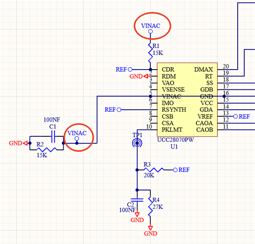
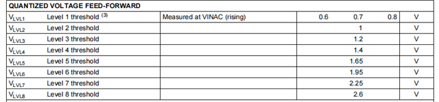
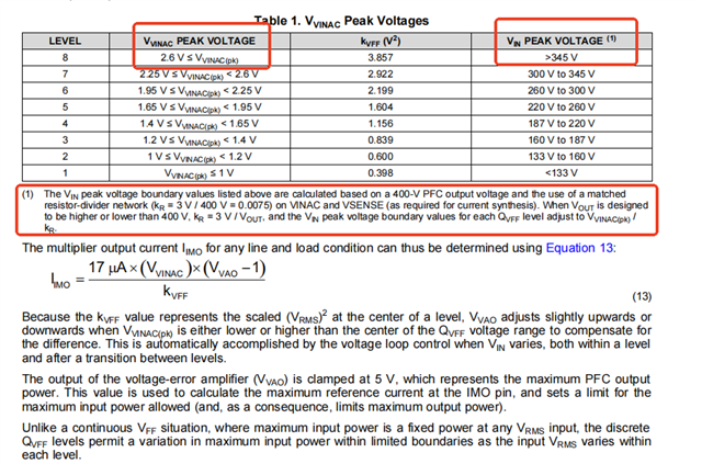
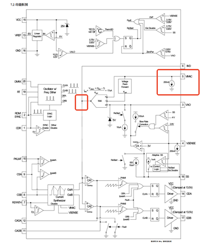
A great benefit of the QVFF architecture is that the fixed kVFF factors eliminate any contribution to distortion of the multiplier output, unlike an externally-filtered VINAC signal which unavoidably contains 2nd-harmonic distortion components. Furthermore, the QVFF algorithm allows for rapid response to both increasing and decreasing changes in input rms voltage so that disturbances transmitted to the PFC output are minimized. 5% hysteresis in the level thresholds help avoid chattering between QVFF levels for VVINAC voltage peaks near a particular threshold or containing mild ringing or distortion. The QVFF architecture requires that the input voltage be largely sinusoidal, and relies on detecting zero-crossings to adjust QVFF downward on decreasing input voltage. Zerocrossings are defined as VVINAC falling below 0.7 V for at least 50 μs, typically.