If you have a related question, please click the "Ask a related question" button in the top right corner. The newly created question will be automatically linked to this question.
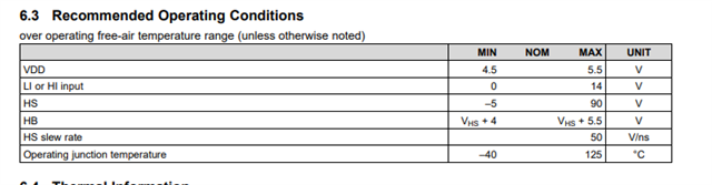
7.3.1 Input and Output The input pins of the LM5113-Q1 are independently controlled with TTL input thresholds and can withstand voltages up to 12 V regardless of the VDD voltage. This allows the inputs to be directly connected to the outputs of an analog PWM controller with up to 12-V power supply, eliminating the need for a buffer stage The output pulldown and pullup resistance of LM5113-Q1 is optimized for enhancement mode GaN FETs to achieve high frequency and efficient operation. The 0.6-Ω pulldown resistance provides a robust low impedance turnoff path necessary to eliminate undesired turnon induced by high dv/dt or high di/dt. The 2.1-Ω pullup resistance helps reduce the ringing and over-shoot of the switch node voltage. The split outputs of the LM5113- Q1 offer flexibility to adjust the turnon and turnoff speed by independently adding additional impedance in either the turnon path, the turnoff path, or both. If the input signal for either of the two channels, HI or LI, is not used, the control pin must be tied to either VDD or VSS. These inputs must not be left floating.