

Part Number: LM74910-Q1
Hi, Engineers,
I use a LM74910 for my board, and the principle is as shown in the figure. The input voltage is connected to the A pin and the voltage is 28V. Now when I give EN and SLEEP high levels, DGATE is only 3.5V higher than A's level (9.5~14V is recommend in the manual); And HGATE is normal, 12V higher than OUT. VCAP capacitors also have a 12V dropout across the two sides, it means that Vcap to VS is 12V.
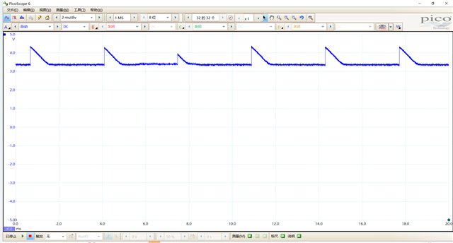
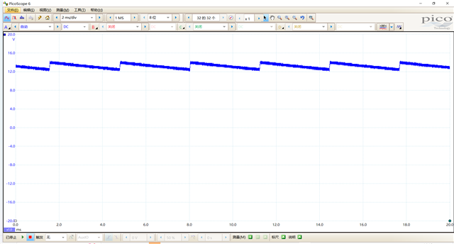
Later, I grounded ILIM and TMR and left IMON and ISCP floating, turned off the diagnostic function, changed the resistance of the NMOS gate to 0, and changed the VCAP capacitance from 100nF to 220nF, 320nF, 670nF, 1uF and so on (the Ciss of two MOS is 10^4 pF). DGATE to A is still 3.5V. Is it normal for DGATE to A to only 3.5V. Then I removed the resistor of the NMOS gate and DGATE to A became 12V. I keep changing the capacitance value of the VCAP and the series resistance of the NMOS gate, no matter how I change it, as long as there is NMOS, then the DGATE to A is about 3.5V.
Senior engineers, can you please help me analyze why DGATE to A can't be in the range of 9~14V as described in the manual?
Hi,工程师们:
我的板子用了个LM74910,原理如图。输入电压连接到A引脚,电压是28V。现在我给EN和SLEEP高电平后,DGATE比A的电平只高出3.5V(手册里是9.5~14V);而HGATE是正常的,比OUT高12V。VCAP电容两端也有12V压差。
后来我把ILIM、TMR接地,IMON、ISCP悬空,关闭了诊断功能,MOS栅极的电阻也换成了0的,也将VCAP电容从100nF换成了220nF、320nF、670nF、1uF等值(其中两个MOS的Ciss是10^4 pF)。DGATE to A还是3.5V。然后我移除了 NMOS 栅极的串联电阻,DGATE to A 变为12V。我不断改变 VCAP 的电容值和 NMOS 栅极的串联电阻,但无论我怎么改变,只要有 NMOS的存在,DGATE to A 的电压大约是3.5V。
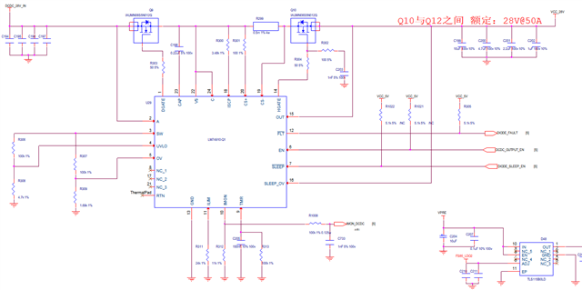
principle
DGATE
charge pump
