

When it comes to MOS transistors, everyone knows about NMOS and PMOS.
So how can we tell the difference between them?
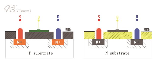
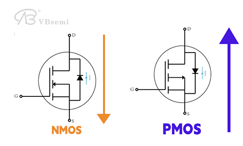
The biggest distinction lies in their substrate structure.
In circuit diagrams, NMOS has a P-type substrate, while PMOS has an N-type substrate.
This is the most intuitive method of differentiation.
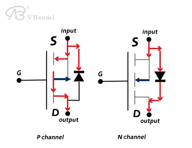
Forms of NMOS and PMOS switching circuits:
NMOS conducts at high level and turns off at low level.
PMOS: Conducts at low level and turns off at high level.
Summary: Conduction condition is high for N and low for P.
Direction of the arrow in circuit symbols:
The arrow pointing towards the gate (G) indicates an N-channel.
The arrow pointing away from the gate (G) indicates a P-channel.
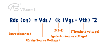
On-resistance:
NMOS: Has a lower on-resistance, suitable for rapid switching operations.
PMOS: Has a higher on-resistance, resulting in slower switching speeds.
Both NMOS and PMOS have an on-resistance after conduction, leading to conduction loss.
Rds(on) = Vds / (k(Vgs - Vth)^2)
Direction of current:
For NMOS, it flows from the drain (D) to the source (S).
For PMOS, it flows in the opposite direction, from S to D.
The appearance of NMOS and PMOS can sometimes be distinguished by visual inspection.
Typically, the die of an NMOS is darker, appearing gray or black, while the die of a PMOS is lighter, appearing pale yellow or pale blue.
NMOS: Usually has a layer of metal (such as tungsten or copper) covering the oxide film.
PMOS: Usually has a layer of insulating material (such as silicon nitride or alumina) covering the oxide film.
By mastering any one of these points, we can distinguish between NMOS and PMOS.
