This thread has been locked.
If you have a related question, please click the "Ask a related question" button in the top right corner. The newly created question will be automatically linked to this question.
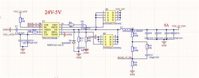
以上这是原理图,请问是有什么设计上的问题吗
您好
已经收到了您的案例,调查需要些时间,感谢您的耐心等待
1.输出传感位置在哪里? 是否在输出盖处? 传感位置和测量位置是否相同。
2.如果出现数据表中提到的OCL状态,可能会出现压降
您好1.输出传感是问输出FB位置吗?
2.ocl这边设定的是Iocl=(9-5)*5/(2*1*0.5*9)+125/6.1=~22.7A
转换器,如果测量位置与调节点不同,则调节传感位置的输出,您可能会看到PCB轨迹导致的下降。 您可以提供布局,SW节点波形,VFB波形吗? 我还注意到C14比我们一般预期的要大。
好的,感谢