请问下 load using QSPI 方式烧录固件,固件是load在CPU的内部flash里面还是外接的flash芯片里呢?如果是load在外接的flash芯片里,请问下默认的是用QSPI的哪种模式呢?另外,
rtclk信号在硬件上是否是必须连接的?为连接的话是否影响load using QSPI,导致load失败?感谢解答以上疑问
This thread has been locked.
If you have a related question, please click the "Ask a related question" button in the top right corner. The newly created question will be automatically linked to this question.
TDA3x芯片里没有flash,需要外接SPI flash存放代码。
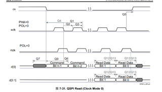
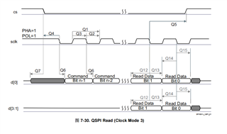
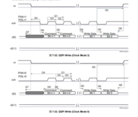
QSPI有两种boot模式QSPI_1: 1-bit SPI flash memories和QSPI_4: 4-bit (Quad) SPI flash memories,看外接的spi flash符合哪种。QSPI boot使用mode 3,rtclk不需要接。请看一下TRM的Table 25-9. Pin Multiplexing According to Boot Interface
25.8.4 SPI/QSPI Flash Devices
https://www.ti.com/lit/ug/spruie7d/spruie7d.pdf
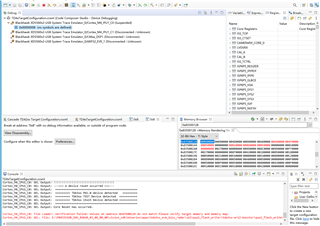
如您所述,我们目前采用QSPI1方式进行load,外接flash芯片采用与开发板相同的型号,但是无法成功烧录,反复报以下两类错误,请根据日志帮忙分析下故障原因,非常感谢!
一、
Cortex_M4_IPU1_C0: GEL Output: --->>> TDA3xx Cortex M4 Startup Sequence In Progress... <<<---
Cortex_M4_IPU1_C0: GEL Output: --->>> TDA3xx Cortex M4 Startup Sequence DONE! <<<---
Cortex_M4_IPU1_C1: GEL Output: --->>> TDA3xx Cortex M4 Startup Sequence In Progress... <<<---
Cortex_M4_IPU1_C1: GEL Output: --->>> TDA3xx Cortex M4 Startup Sequence DONE! <<<---
ARP32_EVE_1: GEL Output: --->>> Configuring EVE Memory Map <<<---
ARP32_EVE_1: GEL Output: --->>> EVE Memory Map Done! <<<---
Cortex_M4_IPU1_C0: GEL Output: --->>> TDA3xx Target Connect Sequence Begins ... <<<---
Cortex_M4_IPU1_C0: GEL Output: --->>> A device reset occurred <<<---
Cortex_M4_IPU1_C0: GEL Output: ==================================================
Cortex_M4_IPU1_C0: GEL Output: ========= TDA3xx PG3.0 device detected =========
Cortex_M4_IPU1_C0: GEL Output: ========= TDA3xx GP Device detected ===========
Cortex_M4_IPU1_C0: GEL Output: ========= TDA3xx 15x15 Device detected ===========
Cortex_M4_IPU1_C0: GEL Output: ==================================================
Cortex_M4_IPU1_C0: GEL Output: Core Reset has occurred.
Cortex_M4_IPU1_C0: GEL Output: ==================================================
Cortex_M4_IPU1_C0: GEL Output: ========= TDA3xx PG3.0 device detected =========
Cortex_M4_IPU1_C0: GEL Output: ========= TDA3xx GP Device detected ===========
Cortex_M4_IPU1_C0: GEL Output: ========= TDA3xx 15x15 Device detected ===========
Cortex_M4_IPU1_C0: GEL Output: ==================================================
Cortex_M4_IPU1_C0: GEL Output: --->>> All Control module lock registers are UNLOCKED <<<---
Cortex_M4_IPU1_C0: GEL Output: --->>> RTI is not currently enabled, so not doing anything <<<---
Cortex_M4_IPU1_C0: GEL Output: --->>> Starting IPU A-MMU configurations... <<<---
Cortex_M4_IPU1_C0: GEL Output: --->>> IPU A-MMU configuration completed. <<<---
Cortex_M4_IPU1_C0: GEL Output: ------------------------------------------------------------------------------------------
Cortex_M4_IPU1_C0: GEL Output: --->>> DDR and DPLL configuration Based on Package selection pin status(Sysboot[7]) <<<---
Cortex_M4_IPU1_C0: GEL Output: ------------------------------------------------------------------------------------------
Cortex_M4_IPU1_C0: GEL Output: --->>> 15x15 Package Detected(SYSBOOT[7]=0)... <<<---
Cortex_M4_IPU1_C0: GEL Output: --->>> PRCM Clock Configuration for OPPNOM in progress... <<<---
Cortex_M4_IPU1_C0: GEL Output: --->>> CORE DPLL OPP 0 clock config is in progress...
Cortex_M4_IPU1_C0: GEL Output: --->>> CORE DPLL OPP 0 is DONE!
Cortex_M4_IPU1_C0: GEL Output: --->>> PER DPLL OPP 0 clock config in progress...
Cortex_M4_IPU1_C0: GEL Output: --->>> PER DPLL OPP 0 is DONE!
Cortex_M4_IPU1_C0: GEL Output: --->>> DSP_GMAC DPLL OPP 0 clock config is in progress...
Cortex_M4_IPU1_C0: GEL Output: --->>> DSP_GMAC DPLL OPP 0 is DONE!
Cortex_M4_IPU1_C0: GEL Output: --->>> EVE_VID_DSP DPLL OPP 0 clock config is in progress...
Cortex_M4_IPU1_C0: GEL Output: --->>> EVE_VID_DSP_DPLL OPP 0 is DONE!
Cortex_M4_IPU1_C0: GEL Output: --->>> PRCM Clock Configuration for OPP 0 is DONE! <<<---
Cortex_M4_IPU1_C0: GEL Output: --->>> PRCM Configuration for all modules in progress... <<<---
Cortex_M4_IPU1_C0: GEL Output: --->>> PRCM Configuration for all modules is DONE! <<<---
Cortex_M4_IPU1_C0: GEL Output: --->>> DDR3 initialization starts (TI 15x15 EVM)... <<<---
Cortex_M4_IPU1_C0: GEL Output: --->>> DDR3 Initialization is in progress ... <<<---
Cortex_M4_IPU1_C0: GEL Output: --->>> DDR DPLL clock config for 532MHz is in progress...
Cortex_M4_IPU1_C0: GEL Output: --->>> DDR DPLL clock config for 532MHz is in DONE!
Cortex_M4_IPU1_C0: GEL Output: Launch full leveling
Cortex_M4_IPU1_C0: GEL Output: Updating slave ratios in PHY_STATUSx registers
Cortex_M4_IPU1_C0: GEL Output: as per HW leveling output
Cortex_M4_IPU1_C0: GEL Output: HW leveling is now disabled. Using slave ratios from
Cortex_M4_IPU1_C0: GEL Output: PHY_STATUSx registers
Cortex_M4_IPU1_C0: GEL Output: --->>> DDR3 532MHz Initialization is DONE! <<<---
Cortex_M4_IPU1_C0: GEL Output: --->>> TDA3xx Begin All Pad Configuration for Vision Platform <<<---
Cortex_M4_IPU1_C0: GEL Output: --->>> TDA3xx Begin All Pad Configuration for RGMII usage on EVM Platform <<<---
Cortex_M4_IPU1_C0: GEL Output: --->>> TDA3xx Begin GMAC_SW MDIO Pad Configuration <<<---
Cortex_M4_IPU1_C0: GEL Output: --->>> TDA3xx End GMAC_SW MDIO Pad Configuration <<<---
Cortex_M4_IPU1_C0: GEL Output: --->>> TDA3xx Begin GMAC_SW RGMII0 Pad Configuration <<<---
Cortex_M4_IPU1_C0: GEL Output: --->>> TDA3xx End GMAC_SW RGMII0 Pad Configuration <<<---
Cortex_M4_IPU1_C0: GEL Output: --->>> TDA3xx End All Pad Configuration for RGMII usage on EVM Platform <<<---
Cortex_M4_IPU1_C0: GEL Output: --->>> TDA3xx End All Pad Configuration for Vision Platform <<<---
Cortex_M4_IPU1_C0: GEL Output: --->>> TDA3xx Target Connect Sequence DONE !!!!! <<<---
Cortex_M4_IPU1_C0: GEL Output: !!!!!!!!!!!!!!!!!!!!!!!!!!!!!!!!!!!!!
Cortex_M4_IPU1_C0: GEL Output: For STM based tracing on TI EVMs,
Cortex_M4_IPU1_C0: GEL Output: run 'TDA3x EVM I2C EXPANDER CONTROL -> Enable_Trace_Pins()' function from Scripts menu on M4/CS_DAP_DebugSS
Cortex_M4_IPU1_C0: GEL Output: !!!!!!!!!!!!!!!!!!!!!!!!!!!!!!!!!!!!!
Cortex_M4_IPU1_C0: GEL Output: Core Reset has occurred.
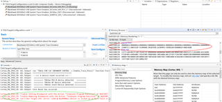
Cortex_M4_IPU1_C0: File Loader: Verification failed: Values at address 0x83500128 do not match Please verify target memory and memory map.
Cortex_M4_IPU1_C0: GEL: File: E:\ti\PROCESSOR_SDK_RADAR_03_08_00_00\vision_sdk\binaries_2243ES1.0-TDA3x\apps\tda3xx_evm_bios_radar\sbl\qspi_flash_writer\tda3xx-ar12-booster\qspi_flash_writer_ipu1_0_release.xem4: a data verification error occurred, file load failed.
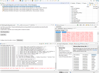
二、
Cortex_M4_IPU1_C0: GEL Output: --->>> TDA3xx Cortex M4 Startup Sequence In Progress... <<<---
Cortex_M4_IPU1_C0: GEL Output: --->>> TDA3xx Cortex M4 Startup Sequence DONE! <<<---
Cortex_M4_IPU1_C1: GEL Output: --->>> TDA3xx Cortex M4 Startup Sequence In Progress... <<<---
Cortex_M4_IPU1_C1: GEL Output: --->>> TDA3xx Cortex M4 Startup Sequence DONE! <<<---
ARP32_EVE_1: GEL Output: --->>> Configuring EVE Memory Map <<<---
ARP32_EVE_1: GEL Output: --->>> EVE Memory Map Done! <<<---
Cortex_M4_IPU1_C0: GEL Output: --->>> TDA3xx Target Connect Sequence Begins ... <<<---
Cortex_M4_IPU1_C0: GEL Output: --->>> A device reset occurred <<<---
Cortex_M4_IPU1_C0: GEL Output: ==================================================
Cortex_M4_IPU1_C0: GEL Output: ========= TDA3xx PG3.0 device detected =========
Cortex_M4_IPU1_C0: GEL Output: ========= TDA3xx GP Device detected ===========
Cortex_M4_IPU1_C0: GEL Output: ========= TDA3xx 15x15 Device detected ===========
Cortex_M4_IPU1_C0: GEL Output: ==================================================
Cortex_M4_IPU1_C0: GEL Output: Core Reset has occurred.
Cortex_M4_IPU1_C0: GEL Output: ==================================================
Cortex_M4_IPU1_C0: GEL Output: ========= TDA3xx PG3.0 device detected =========
Cortex_M4_IPU1_C0: GEL Output: ========= TDA3xx GP Device detected ===========
Cortex_M4_IPU1_C0: GEL Output: ========= TDA3xx 15x15 Device detected ===========
Cortex_M4_IPU1_C0: GEL Output: ==================================================
Cortex_M4_IPU1_C0: GEL Output: --->>> All Control module lock registers are UNLOCKED <<<---
Cortex_M4_IPU1_C0: GEL Output: --->>> RTI is not currently enabled, so not doing anything <<<---
Cortex_M4_IPU1_C0: GEL Output: --->>> Starting IPU A-MMU configurations... <<<---
Cortex_M4_IPU1_C0: GEL Output: --->>> IPU A-MMU configuration completed. <<<---
Cortex_M4_IPU1_C0: GEL Output: ------------------------------------------------------------------------------------------
Cortex_M4_IPU1_C0: GEL Output: --->>> DDR and DPLL configuration Based on Package selection pin status(Sysboot[7]) <<<---
Cortex_M4_IPU1_C0: GEL Output: ------------------------------------------------------------------------------------------
Cortex_M4_IPU1_C0: GEL Output: --->>> 15x15 Package Detected(SYSBOOT[7]=0)... <<<---
Cortex_M4_IPU1_C0: GEL Output: --->>> PRCM Clock Configuration for OPPNOM in progress... <<<---
Cortex_M4_IPU1_C0: GEL Output: --->>> CORE DPLL OPP 0 clock config is in progress...
Cortex_M4_IPU1_C0: GEL Output: --->>> CORE DPLL OPP 0 is DONE!
Cortex_M4_IPU1_C0: GEL Output: --->>> PER DPLL OPP 0 clock config in progress...
Cortex_M4_IPU1_C0: GEL Output: --->>> PER DPLL OPP 0 is DONE!
Cortex_M4_IPU1_C0: GEL Output: --->>> DSP_GMAC DPLL OPP 0 clock config is in progress...
Cortex_M4_IPU1_C0: GEL Output: --->>> DSP_GMAC DPLL OPP 0 is DONE!
Cortex_M4_IPU1_C0: GEL Output: --->>> EVE_VID_DSP DPLL OPP 0 clock config is in progress...
Cortex_M4_IPU1_C0: GEL Output: --->>> EVE_VID_DSP_DPLL OPP 0 is DONE!
Cortex_M4_IPU1_C0: GEL Output: --->>> PRCM Clock Configuration for OPP 0 is DONE! <<<---
Cortex_M4_IPU1_C0: GEL Output: --->>> PRCM Configuration for all modules in progress... <<<---
Cortex_M4_IPU1_C0: GEL Output: --->>> PRCM Configuration for all modules is DONE! <<<---
Cortex_M4_IPU1_C0: GEL Output: --->>> DDR3 initialization starts (TI 15x15 EVM)... <<<---
Cortex_M4_IPU1_C0: GEL Output: --->>> DDR3 Initialization is in progress ... <<<---
Cortex_M4_IPU1_C0: GEL Output: --->>> DDR DPLL clock config for 532MHz is in progress...
Cortex_M4_IPU1_C0: GEL Output: --->>> DDR DPLL clock config for 532MHz is in DONE!
Cortex_M4_IPU1_C0: GEL Output: Launch full leveling
Cortex_M4_IPU1_C0: GEL Output: Updating slave ratios in PHY_STATUSx registers
Cortex_M4_IPU1_C0: GEL Output: as per HW leveling output
Cortex_M4_IPU1_C0: GEL Output: HW leveling is now disabled. Using slave ratios from
Cortex_M4_IPU1_C0: GEL Output: PHY_STATUSx registers
Cortex_M4_IPU1_C0: GEL Output: --->>> DDR3 532MHz Initialization is DONE! <<<---
Cortex_M4_IPU1_C0: GEL Output: --->>> TDA3xx Begin All Pad Configuration for Vision Platform <<<---
Cortex_M4_IPU1_C0: GEL Output: --->>> TDA3xx Begin All Pad Configuration for RGMII usage on EVM Platform <<<---
Cortex_M4_IPU1_C0: GEL Output: --->>> TDA3xx Begin GMAC_SW MDIO Pad Configuration <<<---
Cortex_M4_IPU1_C0: GEL Output: --->>> TDA3xx End GMAC_SW MDIO Pad Configuration <<<---
Cortex_M4_IPU1_C0: GEL Output: --->>> TDA3xx Begin GMAC_SW RGMII0 Pad Configuration <<<---
Cortex_M4_IPU1_C0: GEL Output: --->>> TDA3xx End GMAC_SW RGMII0 Pad Configuration <<<---
Cortex_M4_IPU1_C0: GEL Output: --->>> TDA3xx End All Pad Configuration for RGMII usage on EVM Platform <<<---
Cortex_M4_IPU1_C0: GEL Output: --->>> TDA3xx End All Pad Configuration for Vision Platform <<<---
Cortex_M4_IPU1_C0: GEL Output: --->>> TDA3xx Target Connect Sequence DONE !!!!! <<<---
Cortex_M4_IPU1_C0: GEL Output: !!!!!!!!!!!!!!!!!!!!!!!!!!!!!!!!!!!!!
Cortex_M4_IPU1_C0: GEL Output: For STM based tracing on TI EVMs,
Cortex_M4_IPU1_C0: GEL Output: run 'TDA3x EVM I2C EXPANDER CONTROL -> Enable_Trace_Pins()' function from Scripts menu on M4/CS_DAP_DebugSS
Cortex_M4_IPU1_C0: GEL Output: !!!!!!!!!!!!!!!!!!!!!!!!!!!!!!!!!!!!!
Cortex_M4_IPU1_C0: GEL Output: --->>> A device reset occurred <<<---
Cortex_M4_IPU1_C0: GEL Output: ==================================================
Cortex_M4_IPU1_C0: GEL Output: ========= TDA3xx PG3.0 device detected =========
Cortex_M4_IPU1_C0: GEL Output: ========= TDA3xx GP Device detected ===========
Cortex_M4_IPU1_C0: GEL Output: ========= TDA3xx 15x15 Device detected ===========
Cortex_M4_IPU1_C0: GEL Output: ==================================================
Cortex_M4_IPU1_C0: GEL Output: Core Reset has occurred.
Cortex_M4_IPU1_C0: Can't Run Target CPU: (Error -1268 @ 0x1090001) Device is locked up in Hard Fault or in NMI. Reset the device, and retry the operation. If error persists, confirm configuration, power-cycle the board, and/or try more reliable JTAG settings (e.g. lower TCLK). (Emulation package 9.2.0.00002)
e2e上有个帖子跟您的问题一样,请关注下面的帖子,因为美国是感恩节,回复可能会延时。
https://e2e.ti.com/support/power-management-group/power-management/f/power-management-forum/1055388/tda3xevm-tda3x-ccs-load-program-error-issue