This thread has been locked.

If you have a related question, please click the "Ask a related question" button in the top right corner. The newly created question will be automatically linked to this question.

DAC38RF86: DAC38RF8x GUI and DAC38RF86 Configuration and Finding DAC38RF8x EVMV2.0

Part Number: DAC38RF86

Hi,
Currently using DAC38RF86EVM for signal generator design. However, the following problems are encountered:

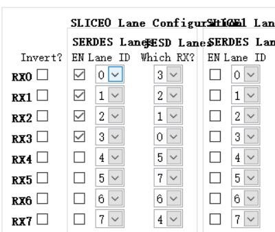
1. the DAC38RF8X EVM GUI V3P1 version of the GUI used, but there is a problem with the GUI display, as shown in Figure, not all of it can be displayed, please ask how to solve this problem;     


2. when using the DAC38RF8X EVM GUI V3P1 version of the GUI configuration, it is found that the value of the corresponding register in the configuration file exported from the GUI is not the same as the set value, the problem may be a problem with that version and may require corresponding optimization;

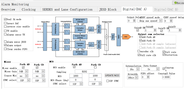
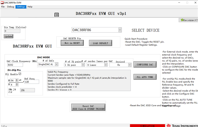
3. when using DAC38RF86, DAC38RF86EVM board clock chip reference clock is 122.88MHz, using DAC on-chip PLL, the reference clock is 128MHz, DAC is 8192MHz, single (DAC A), 4 Lane, interp 8x configuration,as shown in Figure aboveserdes clk for DAC clock 1/4 (DIV = 16, MPY = 0x02 (4x)), found that the channel synchronization on, but no output signal, please what is the problem?

4. In addition, need DAC38RF8X EVM GUI V2.0 version, I wonder if someone can provide.

Thanks!

  • 您好,您的问题我们需要升级到英文论坛看下,有答复尽快给您。

  • 感谢,麻烦了

  • 您看下以下答复:

    1. You may need to either increase or reduce the screen resolution of their pc. These are the only times the tabs get cut off. Under normal operation, we have never seen this before so I am leaning on you needing to play around with screen resolution of their pc.
    2. We have not seen this over many years of using v3.1. I ask you provide an example please.
    3. Is the FPGA link up at FPGA side? To test analog output stage you can enable the NCO and use the constant input mode to have an RF output at the NCO frequency. This will rule out any issue in signal chain.
    4. Providing an earlier release version of this GUI will not resolve the problems you are facing.

    Please uninstall this DAC GUI and reinstall with administrator privileges to see if this resolves all issues.

  • Thank you for your reply:
    1. I adjust my PC resolution, but there is still a problem with the display, whether it is related to the PC system, I am using WIN10 system;


    2. The example as shown. I set LMFSHD=44210,2IQ,16 interpolation,in default,the RX[3:0] is checked. however when I export the configure, in register 0x4A RX[3:0]=0. There are many more such cases.


    3. With the setting LMFSHD=44210,2IQ,16 interpolation,DAC sampling is 81912MHz, set NCO frequency 1000MHz, checke constant,enable NCO and UPDATE NCO,then, export the configure,Configuration data is written to the DAC via the FPGA, however, the DAC has no output. The NCO seting as shown.

    We use Xilinx's FPGAs as well as integrated JESD204B IP. The SYNC LED on the DAC38RF86EVM is lit when the differential SYNC signal of the FPGA to the DAC is single-ended and SYNC is high. It can be seen that the FPGA side and the DAC38RF86 have been synchronized, But no signal output from DAC.


    4、I tried ' uninstall this DAC GUI and reinstall with administrator privileges', but don't valid.

    Now I have some new question:
    The mode of current work is:on chip PLL, single(DAC A), LMFSHD=44210,2IQ,16 interpolation,lane rate 10240MHz, Serdes Configured to Full Rate.
    The data format is shown in the figure,I would like to ask: RX[0]and RX[1]whether the transmitted data is inverted, RX[2]and RX[3] are the same as RX[1]and RX[0]?

  • 好的我们跟进给工程师了。

  • We cannot make any recommendations on how to fix the display issue. This is a windows related issue and not related to our gui as it has been proven to work on many PCs.

    The example as shown. I set LMFSHD=44210,2IQ,16 interpolation,in default,the RX[3:0] is checked. however when I export the configure, in register 0x4A RX[3:0]=0. There are many more such cases.

    What do you mean there are many more such cases? When the export configuration button is pressed all registers are generated, not just modified registers. If the register is the same as the default reset register value then the register will not need to be written to and can simply be ignored.

    With the setting LMFSHD=44210,2IQ,16 interpolation,DAC sampling is 81912MHz, set NCO frequency 1000MHz, checke constant,enable NCO and UPDATE NCO,then, export the configure,Configuration data is written to the DAC via the FPGA, however, the DAC has no output. The NCO seting as shown.

    Please change the data format from 2s complement to offset binary while the constant input button is checked. This should output a waveform at the NCO frequency (in the case above at 1GHz). When using FPGA to transmit data, constant input button should be unchecked and the data format should match whatever format the FPGA is passing into the DAC, whether 2s complement or offset binary.

    The data format is shown in the figure,I would like to ask: RX[0]and RX[1]whether the transmitted data is inverted, RX[2]and RX[3] are the same as RX[1]and RX[0]?

    The data is not inverted. Toggling the lane inversion bit will swap the P and N of the respective RX input.