Other Parts Discussed in Thread: IWR1642,
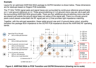
IWR6843ISK有类似 IWR1642的 射频RF天线设计参考文档(如下图所示)么?
IWR 6843ISK 微带线 与 两侧包地间距 多少合适?
Original question:

IWR6843ISK有类似 IWR1642的 射频RF天线设计参考文档(如下图所示)么?
IWR 6843ISK 微带线 与 两侧包地间距 多少合适?