If you have a related question, please click the "Ask a related question" button in the top right corner. The newly created question will be automatically linked to this question.
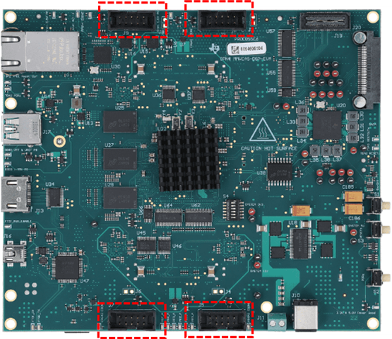
上面的文档里有说明。这个接口可以外接Lattice ECP5 FPGA card。 Included on the EVM is a Lattice Prototyping connector. The interface brings out the VOUT1 interface, I2C5, and two I2C GPIO expander pins to allow for interfacing to a separate Lattice ECP5 FPGA card, which performs VOUT to 10GBase-KR bridging