Other Parts Discussed in Thread: AWRL6432
Dear Engineer
关于AWRL1432 芯片,我在制作电路板上遇到几个问题,如下:
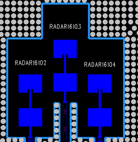
1、在雷达的布局上(如图1),我参考了TI的LAYOUT设计指导,请问雷达天线的加工参数有无特殊要求?
2、请推荐板材,外层成品铜厚和内层成品铜厚。
3、天线外围的过孔过多,能否减少为两排包围天线部分?
4、天线外围的过孔能否使用6/14尺寸的,对过孔的间距和布局能否给一个推荐?
5、芯片的焊盘,在满足贴片的要求上,最小尺寸为多大,DATASHEET中提供的参考为0.26,是否能够更小?
6、我们使用Power Optimized 1.8V I/O Topology作为设计。假设使用1oz的完成铜厚,1.2V和1.8V的线径最小为多少?
Regarding the AWRL1432 chip, I encountered several problems in making the circuit board, as follows:
1. As for the LAYOUT of the radar (as shown in Figure 1), I have referred to the layout design guidance of TI. Are there any special requirements for the processing parameters of the radar antenna?
2. Please recommend the plate, outer finished copper thickness and inner finished copper thickness.
3. There are too many vias around the antenna. Can it be reduced to two rows surrounding the antenna part?
4. Can the vias around the antenna be of 6/14 size? Can you recommend the spacing and layout of the vias?
5. What is the minimum size of the pad of the chip to meet the requirements of the patch? The reference provided in the DATASHEET is 0.26, can it be smaller?
6, we use Power Optimized 1.8V I/O Topology as the design. Assuming 1oz of finished copper thickness is used, what is the minimum wire diameter for 1.2V and 1.8V?
Best Regards

Figure 1
