

Part Number: UNIFLASH
During the development process using the F28P65, the following warning appears when using Uniflash to program, pointing to a memory allocation issue.
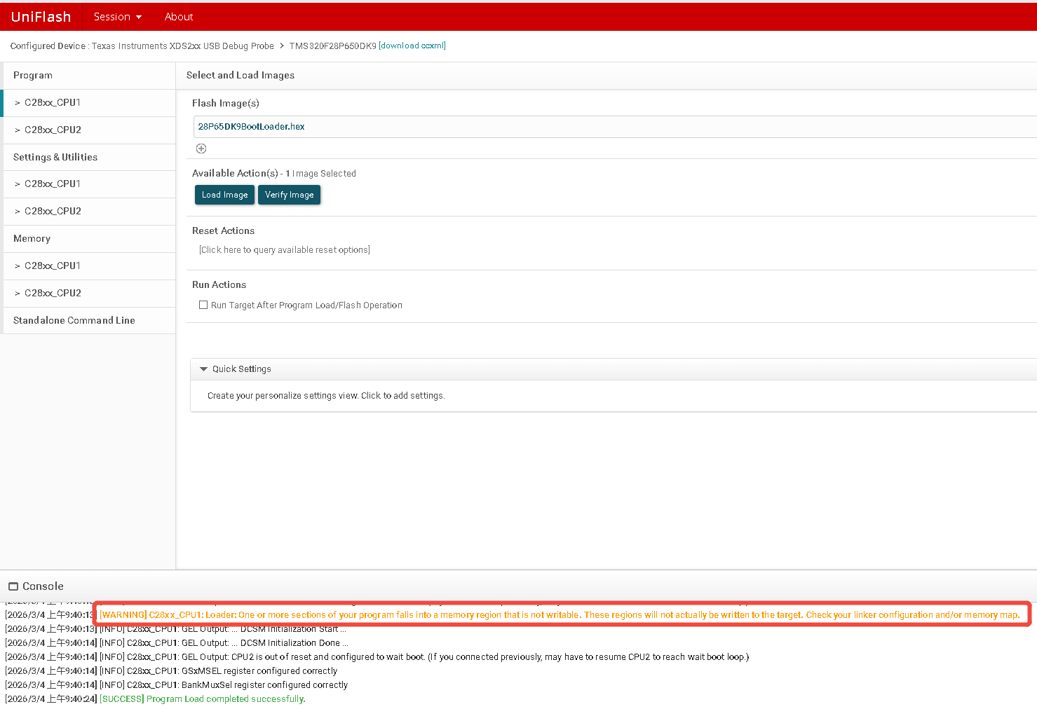
However, after comparing with the datasheet, there are no non-compliant areas, and the program runs normally. Additionally, I only used CPU1. I am somewhat confused about this issue, so I hope to get some answers. Below is the text content of my CMD, hoping it can help in getting assistance:
MEMORY
{
BEGIN : origin = 0x080000, length = 0x00003B
BOOT_RSVD : origin = 0x000002, length = 0x0001AF /* Part of M0, BOOT rom will use this for stack */
RAMM0 : origin = 0x0001B1, length = 0x00024F
RAMM1 : origin = 0x000400, length = 0x000400
RAMD0 : origin = 0x00C000, length = 0x002000
RAMD1 : origin = 0x00E000, length = 0x002000
RAMD2 : origin = 0x01A000, length = 0x002000 // Can be mapped to either CPU1 or CPU2. When configured to CPU2, use the address 0x8000. User should comment/uncomment based on core selection
RAMD3 : origin = 0x01C000, length = 0x002000 // Can be mapped to either CPU1 or CPU2. When configured to CPU2, use the address 0xA000. User should comment/uncomment based on core selection
RAMD4 : origin = 0x01E000, length = 0x002000 // Can be mapped to either CPU1 or CPU2. When configured to CPU2, use the address 0xC000. User should comment/uncomment based on core selection
RAMD5 : origin = 0x020000, length = 0x002000 // Can be mapped to either CPU1 or CPU2. When configured to CPU2, use the address 0xE000. User should comment/uncomment based on core selection
RAMLS0 : origin = 0x008000, length = 0x004000
/*
RAMLS1 : origin = 0x008800, length = 0x000800
RAMLS2 : origin = 0x009000, length = 0x000800
RAMLS3 : origin = 0x009800, length = 0x000800
RAMLS4 : origin = 0x00A000, length = 0x000800
RAMLS5 : origin = 0x00A800, length = 0x000800
RAMLS6 : origin = 0x00B000, length = 0x000800
RAMLS7 : origin = 0x00B800, length = 0x000800
*/
RAMLS8 : origin = 0x022000, length = 0x002000 // When configured as CLA program use the address 0x4000
RAMLS9 : origin = 0x024000, length = 0x002000 // When configured as CLA program use the address 0x6000
// RAMLS8_CLA : origin = 0x004000, length = 0x002000 // Use only if configured as CLA program memory
// RAMLS9_CLA : origin = 0x006000, length = 0x002000 // Use only if configured as CLA program memory
RAMGS0 : origin = 0x010000, length = 0x002000
RAMGS1 : origin = 0x012000, length = 0x002000
RAMGS2 : origin = 0x014000, length = 0x002000
RAMGS3 : origin = 0x016000, length = 0x002000
RAMGS4 : origin = 0x018000, length = 0x002000
#ifdef __TI_COMPILER_VERSION__
#if __TI_COMPILER_VERSION__ >= 20012000
GROUP { /* GROUP memory ranges for crc/checksum of entire flash */
#endif
#endif
/* BEGIN is used for the "boot to Flash" bootloader mode */
// BEGIN : origin = 0x080000, length = 0x000002 // Update the codestart location as needed
/* Flash Banks (128 sectors each) */
CNT00 : origin = 0x08003B, length = 0x000080 /* on-chip FLASH */
FLASH_BANK0 : origin = 0x0800BB, length = 0x17F44 // Can be mapped to either CPU1 or CPU2. User should comment/uncomment based on core selection
FLASHFLAG : origin = 0x097FFF, length = 0x00001
FLASH_BANK0_APP : origin = 0x098000, length = 0x08000
FLASH_BANK1 : origin = 0x0A0000, length = 0x20000 // Can be mapped to either CPU1 or CPU2. User should comment/uncomment based on core selection
FLASH_BANK2 : origin = 0x0C0000, length = 0x20000 // Can be mapped to either CPU1 or CPU2. User should comment/uncomment based on core selection
FLASH_BANK3 : origin = 0x0E0000, length = 0x20000 // Can be mapped to either CPU1 or CPU2. User should comment/uncomment based on core selection
FLASH_BANK4 : origin = 0x100000, length = 0x20000 // Can be mapped to either CPU1 or CPU2. User should comment/uncomment based on core selection
#ifdef __TI_COMPILER_VERSION__
#if __TI_COMPILER_VERSION__ >= 20012000
} crc(_ccs_flash_checksum, algorithm=C28_CHECKSUM_16)
#endif
#endif
CPU1TOCPU2RAM : origin = 0x03A000, length = 0x000400
CPU2TOCPU1RAM : origin = 0x03B000, length = 0x000400
CLATOCPURAM : origin = 0x001480, length = 0x000080
CPUTOCPURAM : origin = 0x001500, length = 0x000080
CLATODMARAM : origin = 0x001680, length = 0x000080
DMATOCLARAM : origin = 0x001700, length = 0x000080
CANA_MSG_RAM : origin = 0x049000, length = 0x000800
CANB_MSG_RAM : origin = 0x04B000, length = 0x000800
RESET : origin = 0x3FFFC0, length = 0x000002
}
SECTIONS
{
codestart : > BEGIN
.text : > FLASH_BANK0, ALIGN(8)
.cinit : > FLASH_BANK0, ALIGN(8)
.switch : > FLASH_BANK0, ALIGN(8)
.reset : > RESET, TYPE = DSECT /* not used, */
.stack : > RAMM1
cnt_00 : > CNT00
.flashflag : > FLASHFLAG
#if defined(__TI_EABI__)
.bss : > RAMLS0
.bss:output : > RAMLS0
.init_array : > FLASH_BANK0, ALIGN(8)
.const : > FLASH_BANK0, ALIGN(8)
.data : > RAMLS0
.sysmem : > RAMLS0
#else
.pinit : > FLASH_BANK0, ALIGN(8)
.ebss : > RAMLS0
.econst : > FLASH_BANK0, ALIGN(8)
.esysmem : > RAMLS0
#endif
ramgs0 : > RAMGS0, type=NOINIT
ramgs1 : > RAMGS1, type=NOINIT
#if defined(__TI_EABI__)
.TI.ramfunc : {} LOAD = FLASH_BANK0,
RUN = RAMLS0,
LOAD_START(RamfuncsLoadStart),
LOAD_SIZE(RamfuncsLoadSize),
LOAD_END(RamfuncsLoadEnd),
RUN_START(RamfuncsRunStart),
RUN_SIZE(RamfuncsRunSize),
RUN_END(RamfuncsRunEnd),
ALIGN(8)
MSGRAM_CPU1_TO_CPU2 > CPU1TOCPU2RAM, type=NOINIT
MSGRAM_CPU1_TO_CPU2_COPY_TO_M1_RAM > CPU1TOCPU2RAM, type=NOINIT
MSGRAM_CPU2_TO_CPU1 > CPU2TOCPU1RAM, type=NOINIT
#else
.TI.ramfunc : {} LOAD = FLASH_BANK0,
RUN = RAMLS0,
LOAD_START(_RamfuncsLoadStart),
LOAD_SIZE(_RamfuncsLoadSize),
LOAD_END(_RamfuncsLoadEnd),
RUN_START(_RamfuncsRunStart),
RUN_SIZE(_RamfuncsRunSize),
RUN_END(_RamfuncsRunEnd),
ALIGN(8)
MSGRAM_CPU1_TO_CPU2 > CPU1TOCPU2RAM, type=NOINIT
MSGRAM_CPU1_TO_CPU2_COPY_TO_M1_RAM > CPU1TOCPU2RAM, type=NOINIT
MSGRAM_CPU2_TO_CPU1 > CPU2TOCPU1RAM, type=NOINIT
#endif
/* crc/checksum section configured as COPY section to avoid including in executable */
.TI.memcrc : type = COPY
}
/*
//===========================================================================
// End of file.
//===========================================================================
*/


