If you have a related question, please click the "Ask a related question" button in the top right corner. The newly created question will be automatically linked to this question.
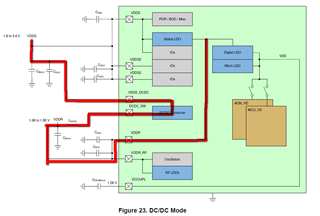
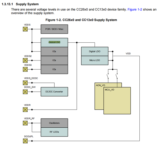
Maximum efficiency is obtained by using the internal DC/DC converter, and it requires an external inductor (LDCDC) and capacitor (CDCDC). The components should be placed as close as possible to the CC13xx/CC26xx device and it is important to have a short current return path for from the CDCDC ground to the pad on the chip (see Section 4.7). In addition, the bulk capacitor on VDDS should be placed close to the VDDS_DCDC-pin. The actual value of LDCDC, CDCDC and CBULK vary from device to device. For the actual values, see the device-specific reference design. When operating in DC/DC mode, the power system dynamically switches between the Global LDO and DC/DC converter depending on the required load to achieve maximum efficiency. If VDDS drops below 2.0 V, the DC/DC converter will be less efficient than the LDO and the device will run in global LDO mode. For systems operating with VDDS less than 2.0 V, consider either global LDO or external regulator mode to save component cost and board area.


 我还是有个疑问,