

Part Number: CC2640R2F
Other Parts Discussed in Thread: CC2642R, LAUNCHXL-CC2640R2, CC2640, CC2640R2L
导入工程“adcsinglechannel ”编译,DEBUG都没有问题,但是代码没有看太明白。
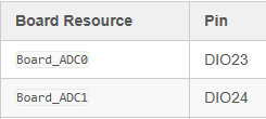
从板载资源来看,ADC0是从DIO23脚输入,ADC1是从DIO24脚输入.
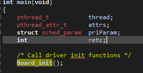
进入main()以后首先执行Board_init();
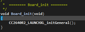
Board_init()又调用CC2640R2_LAUNCHXL_initGeneral();
在CC2640R2_LAUNCHXL_initGeneral();中先执行Power_init();再执行PIN_init();

问题1:Power_init()起什么作用?初始化跟电源相关的资源?但其中似乎又有对时钟的处理。如果在应用程序中没有涉及到电源管理是否可以直接调用不用修改内容?
 *  ======== Power_init ========
 */
int_fast16_t Power_init()
{
    ClockP_Params clockParams;
    uint32_t ccfgLfClkSrc;
    uint32_t timeout;

    /* if this function has already been called, just return */
    if (PowerCC26XX_module.initialized) {
        return (Power_SOK);
    }

#if defined(DeviceFamily_CC26X0R2)
    /* check to see if the JTAG_PD is on, meaning the emulator was attached during boot and */
    /* that the user is in an active debug session */
    PowerCC26XX_module.emulatorAttached = (HWREG(AON_WUC_BASE + AON_WUC_O_PWRSTAT) & AON_WUC_PWRSTAT_JTAG_PD_ON) == AON_WUC_PWRSTAT_JTAG_PD_ON;
#endif

    /* set module state field 'initialized' to true */
    PowerCC26XX_module.initialized = true;

    /* set the module state enablePolicy field */
    PowerCC26XX_module.enablePolicy = PowerCC26XX_config.enablePolicy;

    /* copy the Power policy function to module state */
    PowerCC26XX_module.policyFxn = PowerCC26XX_config.policyFxn;

    /* construct the Clock object for scheduling of wakeups */
    /* initiated and started by the power policy */
    ClockP_Params_init(&clockParams);
    clockParams.period = 0;
    clockParams.startFlag = false;
    clockParams.arg = 0;
    ClockP_construct(&PowerCC26XX_module.clockObj, &emptyClockFunc,
        0, &clockParams);

    /* construct the Clock object for XOSC_HF switching */
    /* initiated and started by Power module when activating XOSC_HF */
    ClockP_construct(&PowerCC26XX_module.xoscClockObj, &switchXOSCHFclockFunc,
        0, &clockParams);

    /* construct the Clock object for disabling LF clock quailifiers */
    /* one shot, auto start, first expires at 100 msec */
    ClockP_construct(&PowerCC26XX_module.lfClockObj, &lfClockReadyCallback,
        0, &clockParams);

    (*(PowerCC26XX_config.calibrateFxn))(PowerCC26XX_SETUP_CALIBRATE);

    DRIVERLIB_ASSERT_CURR_RELEASE();
问题2:PIN_init()中的BoardGpioInitTable没有提及ADC0(DIO23)和ADC1(DIO24),它们的初始化代码在哪里?
const PIN_Config BoardGpioInitTable[] = {

    CC2640R2_LAUNCHXL_PIN_RLED | PIN_GPIO_OUTPUT_EN | PIN_GPIO_LOW | PIN_PUSHPULL | PIN_DRVSTR_MAX,       /* LED initially off */
    CC2640R2_LAUNCHXL_PIN_GLED | PIN_GPIO_OUTPUT_EN | PIN_GPIO_LOW | PIN_PUSHPULL | PIN_DRVSTR_MAX,       /* LED initially off */
    CC2640R2_LAUNCHXL_PIN_BTN1 | PIN_INPUT_EN | PIN_PULLUP | PIN_IRQ_BOTHEDGES | PIN_HYSTERESIS,          /* Button is active low */
    CC2640R2_LAUNCHXL_PIN_BTN2 | PIN_INPUT_EN | PIN_PULLUP | PIN_IRQ_BOTHEDGES | PIN_HYSTERESIS,          /* Button is active low */
    CC2640R2_LAUNCHXL_SPI_FLASH_CS | PIN_GPIO_OUTPUT_EN | PIN_GPIO_HIGH | PIN_PUSHPULL | PIN_DRVSTR_MIN,  /* External flash chip select */
    CC2640R2_LAUNCHXL_UART_RX | PIN_INPUT_EN | PIN_PULLDOWN,                                              /* UART RX via debugger back channel */
    CC2640R2_LAUNCHXL_UART_TX | PIN_GPIO_OUTPUT_EN | PIN_GPIO_LOW | PIN_PUSHPULL,                         /* UART TX via debugger back channel */
    CC2640R2_LAUNCHXL_SPI0_MOSI | PIN_INPUT_EN | PIN_PULLDOWN,                                            /* SPI master out - slave in */
    CC2640R2_LAUNCHXL_SPI0_MISO | PIN_INPUT_EN | PIN_PULLDOWN,                                            /* SPI master in - slave out */
    CC2640R2_LAUNCHXL_SPI0_CLK | PIN_INPUT_EN | PIN_PULLDOWN,                                             /* SPI clock */

    PIN_TERMINATE
};
问题3:
这里定义了SPI0使用的管脚
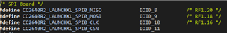
这里将这几个管脚初始化

但IOID_8~IOID_11是如何映射到SPI0外设的?
问题4:看资料介绍同一PIN引脚是可以映射多种功能的,如数字IO、模拟输入等,有没有如何映射的说明?
