

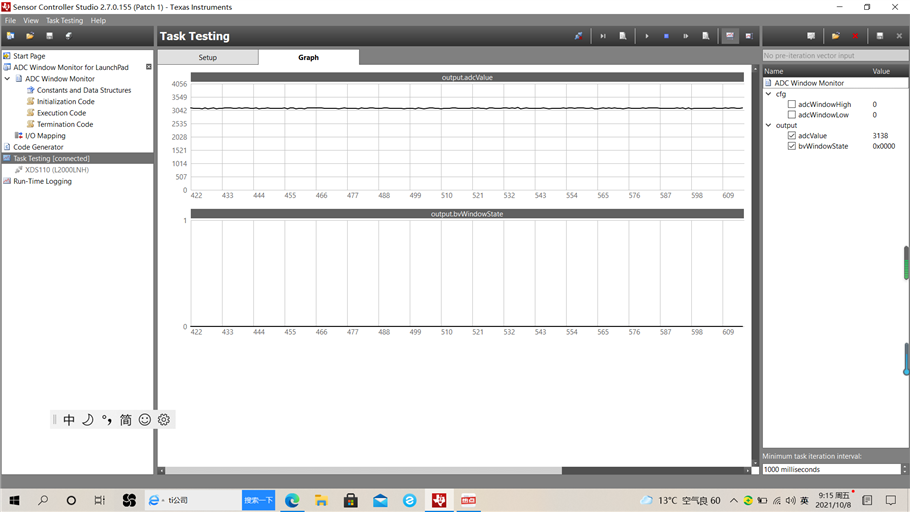
各位专家大家好: 现在我使用SCS 中的ADC Window Monitor for LaunchPad 例程,对AD 输入数据进行分析,当AD IO 接入 3.3 v 引脚时,看到例程中AD 读取的数据是 3100mv , 我用万用表测得的数值是 3.3 V .
这种情况是什么原因造成的。
各位专家大家好: 现在我使用SCS 中的ADC Window Monitor for LaunchPad 例程,对AD 输入数据进行分析,当AD IO 接入 3.3 v 引脚时,看到例程中AD 读取的数据是 3100mv , 我用万用表测得的数值是 3.3 V .
这种情况是什么原因造成的。
