TINA-TI_TRA_CHINESE: opa855:High-Bandwidth TIA Design and Engineering Implementation

Part Number: TINA-TI
Other Parts Discussed in Thread: OPA855

Dear Engineers,

Hello. I am currently designing a 1 GHz-bandwidth transimpedance amplifier (TIA) and plan to implement it using the OPA855 operational amplifier together with a photodiode whose junction capacitance is 0.65 pF. I have carried out simulations in TINA, but I have encountered several points of confusion during the process.

I would sincerely appreciate it if you could offer me some guidance or suggestions. Thank you very much for your time and support.

My questions are as follows:

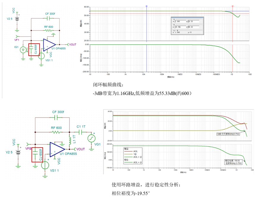
(1) Initially, I assumed that the OPA855 model already included the input capacitance, so I set CJ to represent only the photodiode junction capacitance of 0.65 pF. Under this condition, the AC analysis showed a bandwidth of 1.13 GHz, but the phase margin was only –20°.

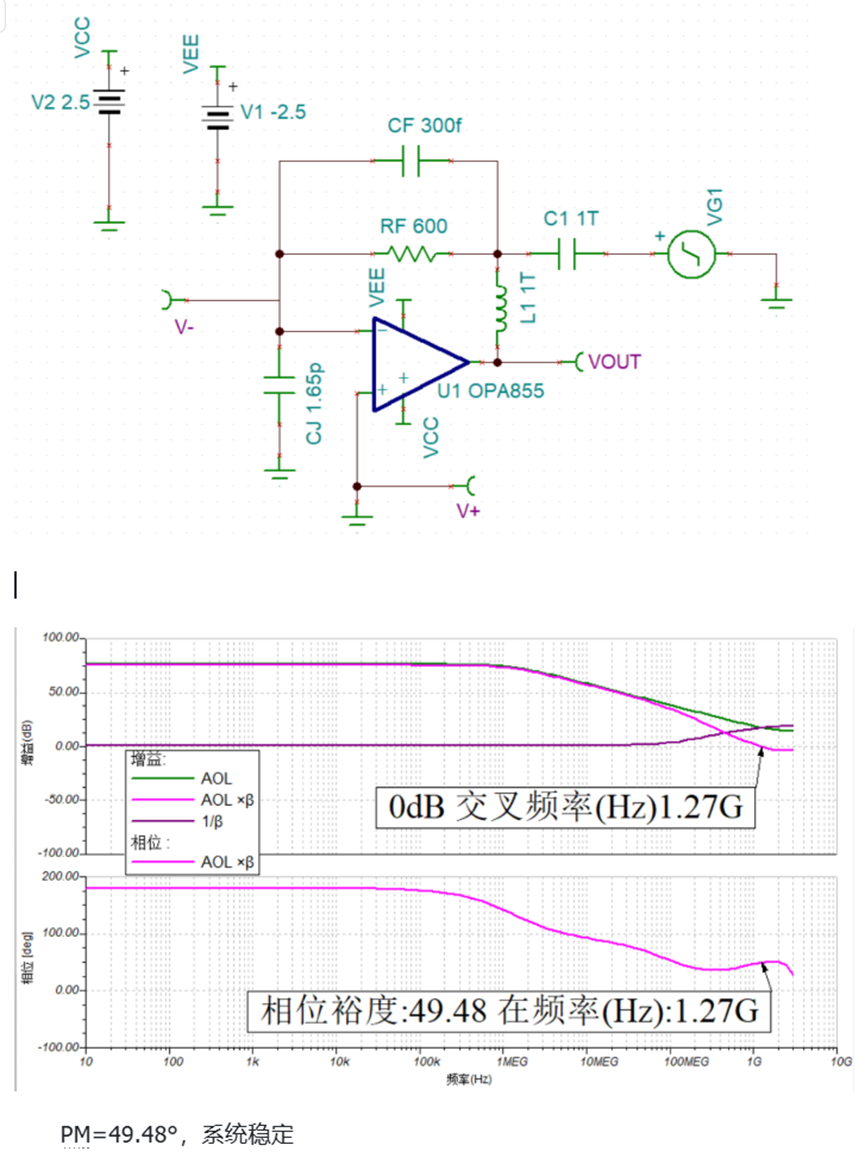
I then increased the capacitance at the junction node to 1.65 pF. With this change, the bandwidth became 1.11 GHz, while the phase margin improved significantly to 50°.

Could you please explain the reason for this behavior?


(2) If the PCB is fabricated according to the schematic I provided, is this design feasible from an engineering perspective? As far as I understand, the parasitic capacitance and inductance of the PCB will significantly affect a transimpedance amplifier. In addition, the capacitance values of 0.3 pF and 1.65 pF are extremely small—especially 0.3 pF. How can such small capacitances be realized in practical hardware?

(3) If my current component selection is not appropriate, I would appreciate any suggestions you could offer.

(4) Is it feasible to achieve a 1 GHz-bandwidth transimpedance amplifier through careful design?


Thanks.

JINGLIN

  • 您好,收到了您的案例,调查需要些时间,感您的耐心等待。

  •   Thank you for the simulations and debugging steps. 

    1. Your thought process here is correct, and the values you have chosen are also the same ones from our TIA calculators for 600Ohm feedback resistor and 0.65pF input photodiode capacitance. The OPA855 model will have the internal capacitance modelled. The reason why increasing the capacitance further at the input stabilizes the circuit is because this amplifier is decompensated. The OPA855 is stable for gains of 7V/V or greater. In a regular voltage feedback amplifier configuration, you would set RF and RG to set the gain to 7V/V or greater. For a TIA, this occurs naturally since noise gain will be 1+C_total_Input/C_Feedback


      With 0.65pF, this would be 1 + 1.4pF/0.3pF = 5.6V/V. When increasing your external input capacitance to 1.65pF, this would be 1 + 1 + 2.4pF/0.3pF = 9V/V. 

      You could add an external capacitor to the input to stabilize the circuit, or you can decrease your feedback capacitor. Both of these would affect bandwidth. 

    2.  Agreed that PCB layout for these high speeds will need very careful PCB design and planning. The usual max possibility to go down to is 0.1pF. The input capacitance will be internal to the photodiode capacitance. We highly recommend adding a DNP (do not place) input capacitance to ground as well at the input of the amplifier for above 1) reason. I have seen methods to decrease feedback capacitance using capacitive t-networks 


      However, when I have seen this implemented, I have seen issues come from this network with increase instability. Therefore, I recommend just placing two series capacitors instead in the feedback with trace length as short as possible. And, of course a separate GND and PWR plane underneath and these planes cutoff right under the input/feedback traces at the amplifier to minimize capacitive parasatics. 

    3. My suggestion is to keep the components but add the DNP input capacitance to ground to add more input capacitance rather than decreasing the feedback capacitance to obtain the required gain for stability. This will decrease bandwidth, but you may be able to achieve 1GHz with tuning. 

    4. It will be difficult and will require very careful PCB planning, but it may be possible based on calc/sims. When PCB layout is done, we can help review it, and I would recommend importing the layout to a simulator that calculates parasatics/impedance. We use Ansys on our end. 

    Thank you,

    Links

  • Thank you very much for your detailed reply and valuable suggestions. After careful consideration and self-review, I have two further questions and would greatly appreciate your guidance.

    (1)From a design trade-off and risk-mitigation perspective, would you recommend populating a fixed external input capacitor (e.g., 1 pF to ground) at the inverting input by default in order to explicitly satisfy the OPA855 minimum stable noise-gain condition (≥ 7 V/V), or is it generally preferable to reserve a DNP input capacitor footprint to ground and populate it only if instability is observed during bench testing?

    In my design, the PCB uses a four-layer stackup (TOP – GND – POWER – BOTTOM), and both the GND and POWER planes have been completely cleared beneath the inverting input node. As a result, the parasitic capacitance associated with a DNP input capacitor footprint is expected to be minimal. Under these conditions, would the DNP-only approach be considered sufficiently robust for first-pass hardware, or would pre-populating the input capacitor still be advisable for margin?

    (2)I will upload my PCB design files for your review. I would appreciate it if you could examine the layout and provide comments or recommendations. In the current PCB layout, neither a populated 1 pF external input capacitor nor a DNP input capacitor to ground is included.

    I look forward to your response.

    TIA_pcb.zip

  • No problem!

      Yes, I agree, you can just add the fixed external input capacitor of 1pF at the inverting pin by default, and during testing you can remove or tune if needed. This way you will satisfy the theoretical calculations for OPA855 min stable noise gain of ≥ 7V/V. 

      Yes, your 4-layer approach is correct. There could be still parasitic capacitance, but due to the cut-off of the inner planes, I agree to keep the default 1pF input capacitance for margin.

      I reviewed your PCB design, I have a couple notes:

    1. I would try to move the PD as close as possible to the input of the amplifier. This is because the longer the trace length, the more parasatic inductance that can be introduced. This means that the trace might isolate the internal capacitor of the PD to the amplifier causing instability. This is why having an external input capacitance is also useful here as well. 
    2. Cutoff of inner layer doesn't have to be too large, it can just be directly underneath the pads of the feedback/inverting input components. 
    3. Adding a input connection to IN+ of the amplifier in-order to bias the amplifier if needed. It seems like you are going with a split-supply approach, which would work without needing to bias. However, adding this might be useful if needed. 

      I adjusted our OPA855 EVM with your components. For some reason directly copying over your diode puts a yellow box around it which is causing collision. I would adjust the PCB file attached to move it even closer to C9 when you import the component correctly if you will be using our PCB file. Also, our PCB file needs to be edited to add the PD"s header net for the different supply or if you will adjust to single 5V supply then to VCC supply. If you will continue with split supply, which actually might be easier during testing. Then you can create a boxed off region for a different supply net on the PWR plane for the PD.

    AMPS032E1.PcbDoc

  • Thank you very much for your previous response. I will revise and further optimize my PCB design in accordance with your suggestions.

    Meanwhile, for the purpose of systematic performance evaluation and characterization of the designed 1-GHz-class transimpedance amplifier (TIA), I plan to carry out measurements covering parasitic parameters, frequency-domain and time-domain characteristics, as well as noise performance. I would like to consult you regarding the following test methodologies.

     (1): Measurement of Parasitic Capacitance

    Is there a method that allows for a more direct and quantitative measurement of the effective parasitic capacitance in a transimpedance amplifier circuit?

    In the literature, I have encountered an indirect approach in which a high-speed pulse (or step) stimulus is applied to the TIA input. The system bandwidth is then estimated from the output signal rise time, and the equivalent parasitic capacitance is inferred accordingly.

    Is this method still feasible and sufficiently accurate for a high-speed TIA with a bandwidth on the order of 1 GHz? In practical engineering applications, are there specific limitations or precautions that must be taken when using this approach?

    (2): Measurement of Bandwidth, Linearity, and Noise

    Can high-speed measurement instruments such as a vector network analyzer (VNA) or a sampling oscilloscope be used to characterize the key performance parameters of a transimpedance amplifier?

    Specifically:

    • Can a VNA be used to measure the –3 dB bandwidth and frequency response of a TIA?

    • Can linearity (e.g., compression behavior or distortion) be evaluated using time-domain or frequency-domain measurement techniques?

    • For noise performance (such as equivalent input current noise or output voltage noise), are there mature and reproducible measurement methods available?

    If these approaches are applicable, are there any recommended or commonly accepted test configurations and measurement procedures?

    (3): Completeness of TIA Performance Evaluation

    When evaluating the performance of a transimpedance amplifier, in addition to commonly reported metrics such as bandwidth and noise, are there other critical parameters that should be carefully tested?

    For example, stability, transient response, dynamic range, or sensitivity to output loading.

    In high-speed (GHz-class) TIA applications, which performance metrics are considered essential from an engineering standpoint but are often overlooked in practice?

    (4): Input Impedance Matching of a Transimpedance Amplifier

    Is input impedance matching required at the input of a transimpedance amplifier?

    In my literature review, I have found extensive discussions on output impedance matching for transimpedance amplifiers, particularly for driving transmission lines or measurement equipment. However, I have been unable to find clear or consistent references addressing input impedance matching for TIA circuits.

    Since the input of a transimpedance amplifier is typically designed to operate as a virtual ground with very low input impedance, it is unclear whether conventional impedance-matching concepts (such as 50-Ω matching) are applicable or even meaningful at the input.

    I would greatly appreciate your insights and recommendations.

  • Hello,

    1. Measurement of Parasitic Capacitance
      1. At these very low capacitance, you will not be able to accurately directly measure the value in practice. The indirect method you have encountered is what we have done as well in the lab. Either we will have different board revisions to minimize parasitic capacitance and check the resulting closed bandwidth and/or we would add an external input capacitor or adjust the feedback capacitance until we reach stability, then tune value for closed-loop bandwidth. This method is feasible at any bandwidth, especially at 1GHz, you would expect to need to do a lot of small incremental tuning at the feedback and input.

    2. Measurement of Bandwidth, Linearity, and Noise
      1. Yes, we use VNAs, oscilloscopes, and spectrum analyzers for characterizing TIAs. 
      2. VNAs can be for frequency response plot. You can also calculate closed-loop bandwidth by looking at the rise time of the output pulse on a high speed, high bit scope. 
      3. Linearity (e.g., compression behavior or distortion) can be evaluated using time-domain measurement via a high speed scope. 
      4. For noise measurement, we use a spectrum analyzer. Here is a quick app note on our exact methodology for this: https://www.ti.com/lit/ug/tidu016/tidu016.pdf?

    3. Completeness of TIA Performance Evaluation 
      1. I recommend to first start with checking the transient response of the device. This will show if there are any obvious instabilities via high frequencies oscillations you would see on the scope. Make sure to keep the cables as short as possible, and have them be 50 ohm impedance matched to avoid power reelections which would show up as ringing on your pulse. Then, as you mentioned, the next would be to look at linearity and range on the scope, then bandwidth via network analyzer or by rise time calculation on the scope, and then noise via spectrum analyzer. Those are the critical specifications for high-speed TIA applications. We have seen others also look at overload recovery in the case of output saturation at your TIA, this is done on the scope. And, some applications also require calculation of the resulting pulse's overshoot/undershoot percentage. 

    4. Input Impedance Matching of a Transimpedance Amplifier
      1. You are correct that input/output impedance matching is required for driving transmission lines or for high speed applications. Input impedance is not required at the input of a TIA since your input is from a current source (PD), ideally to be very high impedance. Impedance matching is required for very high speed applications where source is from a low impedance (voltage) as well as for long distance (trace or cable in relation to speed). You would need to match at the output since you will have a cable to your measurement equipment. And at GHz speeds, this distance is limited to 52.5 mm length. This website is a series on this topic which I found very useful in explaining this concept: link.
      2. Your statement: "Since the input of a transimpedance amplifier is typically designed to operate as a virtual ground with very low input impedance, it is unclear whether conventional impedance-matching concepts (such as 50-Ω matching) are applicable or even meaningful at the input." is correct that it is designed to operate with very low input impedance. However, the second part would not be directly the reason on why impedance matching would not be required. It is due to the answer in part a) where it is a current output and would be directly feeding into the RF (feedback resistor) for voltage conversion. In this case, changing the feedback resistor, or the gain, will not affect the input impedance from the perspective of the source. You want the current to shunt to just the feedback resistor to keep your signal fidelity. Therefore, yes indirectly the entire statement is correct. 
  • Thank you very much for your detailed feedback and guidance. I will follow your recommendations and apply them in my practical implementation and simulation verification.