If you have a related question, please click the "Ask a related question" button in the top right corner. The newly created question will be automatically linked to this question.
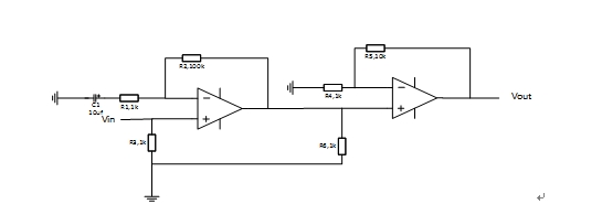
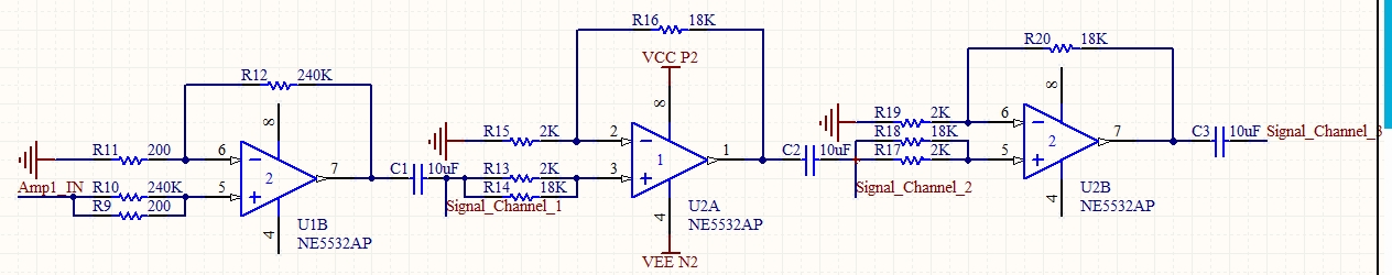
There is no DC path for your coupling capacitor C1 and C2. Bias current from pin3 will charge them up to rail. you need to add resistor between pin3 and GND.
There is no DC path for your coupling capacitor C1 and C2. Bias current from pin3 will charge them up to rail. you need to add resistor between pin3 and GND.


