Part Number: TLV320AIC3204
这是我的寄存器配置
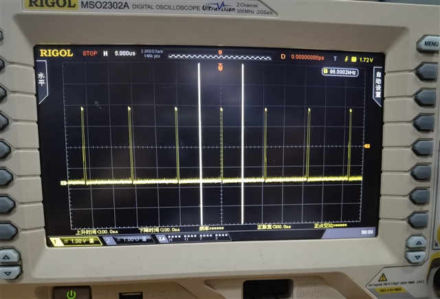
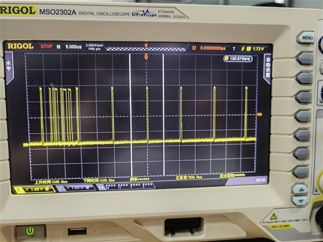
MCLK=24.576MHZ,WCLK=3.072MHZ,BCLK=48KHZ,AIC3204处于主模式,给FPGA提供WCLK和BCLK
# 寄存器 写入数据
0x00,0x00 // Initialize to Page 0
0x01,0x01 // S/W Reset to initialize all registers
0x0b,0x81 // Power up NDAC divider with value 1
0x0c,0x84 // Power up MDAC divider with value 4
0x0d,0X00 // Program OSR for DAC to 128(MSB)
0x0e,0X80 // Program OSR for DAC to 128(LSB)
0x12,0x81 // Power up NADC divider with value 1
0x13,0x84 // Power up MADC divider with value 4
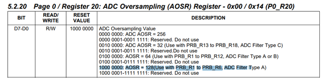
0x14,0x80 // Program OSR for ADC to 128
0x19,0x00 //Select CODEC_CLKIN = MCLK
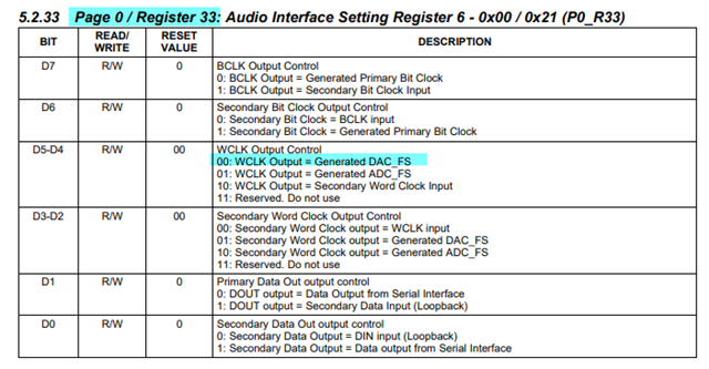
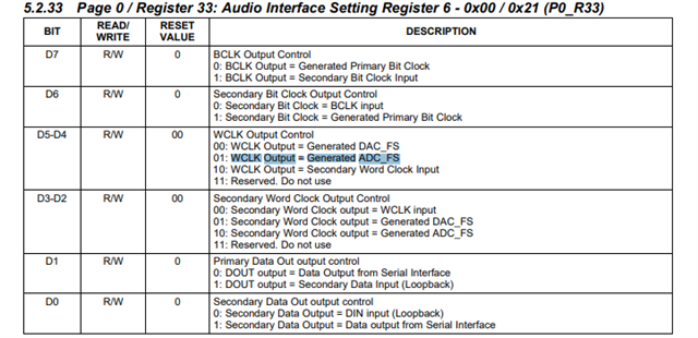
0x1b,0x3c // Set the word length of Audio Interface to 32bits,BCLK,WCLK is output from the device
0x1c, 0x00 // Data Offset = 0 BCLKs
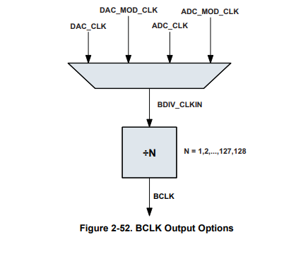
0x1d, 0x06 // BDIV_CLKIN = ADC_CLK
0x1e, 0x88 // Power up BCLK divider with value 8
0x3c,0x04 // Select DAC PRB_P4
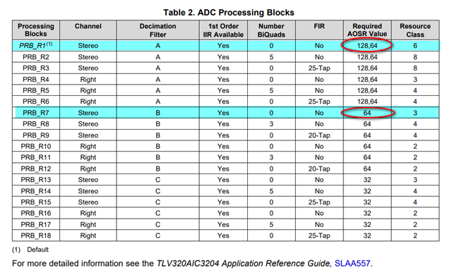
0x3d,0x01 // Select ADC PRB_R1
0x00,0x01 // Select Page 1
0x01,0x08 // Disable Internal Crude AVdd in presence of external AVdd supply or before powering up internal AVdd LDO
0x02,0x00 // Enable Master Analog Power Control
0x14,0x25 //HP soft stepping settings for optimal pop performance at power up
//Rpop used is 6k with N = 6 and soft step = 20usec. This should work with 47uF coupling
//capacitor. Can try N=5,6 or 7 time constants as well. Trade-off delay vs “pop” sound.
0x0a,0x00 // Set the input common mode to 0.9V
/*---Analog Routing---*/
0x0c,0x08 //Route Left DAC to HPL
0x0d,0x08 //Route Right DAC to HPR
0x0e,0x08 //Route Left DAC to LOL
0x0f,0x08 //Route Right DAC to LOR
0x03,0x00 //Set the DAC PTM mode to PTM_P3/4
0x04,0x00 //Set the DAC PTM mode to PTM_P3/4
0x3d,0x00 // Select ADC PTM_R4
0x10,0x00 //Set the HPL gain to 0dB
0x11,0x00 //Set the HPR gain to 0dB
0x12,0x00 //Set the LOL gain to 0dB
0x13,0x00 //Set the LOR gain to 00dB
0x09,0x3c //Power up HPL and HPR, LOL and LOR drivers
//Wait for 2.5 sec for soft stepping to take effect
//Else read Page 1, Register 63d, D(7:6). When = “11” soft-stepping is complete
0x47,0x31 // Set MicPGA startup delay to 3.1ms
0x7b,0x01 // Set the REF charging time to 40ms
0x34,0x80 // Route IN1L to LEFT_P with 20K input impedance
0x36,0x80 // Route Common Mode to LEFT_M with impedance of 20K
0x37,0x80 // Route IN1R to RIGHT_P with input impedance of 20K
0x39,0x80 // Route Common Mode to RIGHT_M with impedance of 20K
0x3b,0x0c // Unmute Left MICPGA, Gain selection of 6dB to make channel gain 0dB
// Register of 6dB with input impedance of 20K => Channel Gain of 0dB
0x3c,0x0c // Unmute Right MICPGA, Gain selection of 6dB to make channel gain 0dB
// Register of 6dB with input impedance of 20K => Channel Gain of 0dB
0x00,0x00 // Select Page 0
0x3f,0xd6 //Power up the Left and Right DAC Channels with route the Left Audio digital data to
//Left Channel DAC and Right Audio digital data to Right Channel DAC
0x40,0x00 //Unmute the DAC digital volume control and enable syncronized control (use L-ch)
0x51,0xc0 // Power up Left and Right ADC Channels
0x52,0x00 // Unmute Left and Right ADC Digital Volume Control.