If you have a related question, please click the "Ask a related question" button in the top right corner. The newly created question will be automatically linked to this question.
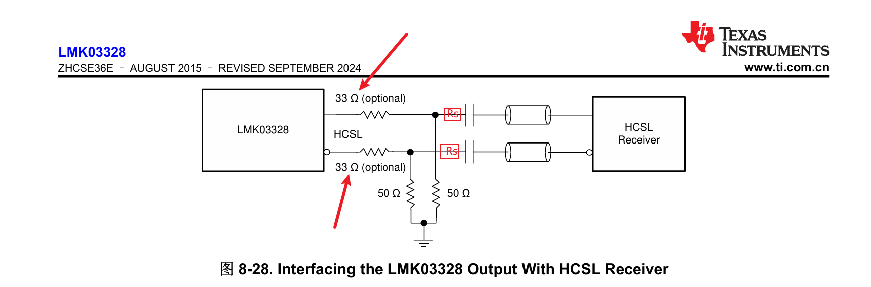
The HCSL output structure is open-drain and can be direct coupled or AC coupled to HCSL receivers with appropriate termination scheme. This output structure supports either on-chip 50-Ω termination or off-chip 50-Ω termination. The on-chip, 50-Ω termination is provided primarily for convenience when driving short traces. In the case of driving long traces possibly through a connector, the on-chip termination must be disabled and a 50 Ω to GND termination at the receiver must be implemented. The output supplies can be operated from 1.8 V, 2.5 V, or 3.3 V without any impact on jitter performance or other AC or DC specifications. The LVCMOS outputs on each side (P and N) can be configured individually to be complementary or in-phase or can be turned off (high output impedance). The LVCMOS outputs are always at 1.8-V logic level irrespective of the output supply. In case 3.3-V LVCMOS outputs are required, STATUS1 and/or STATUS0 can be configured as 3.3-V LVCMOS outputs.